How Photonic Chips Differ From Electronic Chips
Light carries data across a building for a small fraction of the energy that copper needs to do the same job. It is also slower than copper over the short hops on a circuit board, it cannot be held still and stored the way an electric charge can, and it has never been made into a transistor that works.
Photonic chips are cut from the same polished discs of silicon that processors are cut from, in some cases in the same factories, and yet the job they do is almost entirely different. An electronic chip works by parking electric charge on a tiny patch of silicon, where the presence or absence of that charge stands for a one or a zero, and it switches that charge about using transistors. A photonic chip holds nothing at all, because what it works with is light, and light will not sit still to be held anywhere. It guides a beam along narrow channels etched into silicon and glass, then stamps data onto that beam by altering how bright it is. It can instead alter where the beam sits in its own wave cycle, a property engineers call its phase, before turning the light back into an electric current at the far end.
That one difference decides where each kind of chip is worth having, and it is why the volume market for photonic chips is not computation at all but the far less glamorous business of moving data between machines. The reason that market exists is economic rather than technical, because the cost of pushing bits down a copper wire climbs with distance and with speed, while the cost of sending the same bits as light does not. Optical transceivers are the modules that turn an electrical signal into light at one end of a cable and back into electricity at the other.
LightCounting counts supplier revenue from those and the products sold alongside them at $23.8 billion in 2025, up 55 per cent on the year before. Ethernet transceivers are about $18 billion of that and active optical cables a further $1.1 billion, with the remainder spread across telecom wavelength systems, FibreChannel, wireless and fibre to the home. The 55 per cent rise is LightCounting’s own figure, and it does not publish the 2024 total sitting behind it.
Not all of that money buys a photonic integrated circuit, because a great many modules are built from discrete lasers and detectors instead. The nearest published measure of the share that does is the proportion of transceiver sales built on silicon photonics modulators. LightCounting put that at 33 per cent in 2024 and expects it to pass half in 2026. Even on the lower of those two readings, no other application of integrated photonics comes near it.
Most writing on the subject tells you that photonic chips are faster than electronic ones, which is not merely a loose way of putting things but, in the most literal sense available, the wrong way round. The real advantage is something else entirely, and what follows sets out what these chips actually contain, what the physics genuinely buys, and the three walls that have kept light out of the logic.
A buyer can have the conclusion now. Co-packaged optics in 2026 is a sampling-stage purchase rather than a shipping one, and the vendors say so themselves in their availability sections. Waiting has a price all the same. A 102.4 terabit switch on the old pluggable design draws about 6,400 watts, where the same switch with the optics on its package draws about 4,100. The pluggable one therefore carries about 2.3 kilowatts it did not need to, which is roughly what three H100 boards draw. That surplus costs real money every year, and it is not what decides the purchase, because the part cannot be bought in 2026 at any price. Supply gates delivery here, not the size of the saving. Qualify the technology now, and buy it when the line ships.
- The parts are sized by the wavelength and will not shrink
- Light in silicon is slower than copper on a board
- Distance sets the bill for copper and not for light
- The saving arrives in picojoules per bit
- Miller’s criteria kill optical logic and acquit the accelerator, which loses on area and energy instead
- Area costs Lightmatter’s accelerator seventeen to fifty times at the clock it ran
- Energy per operation turns on a clock Lightmatter’s chip never reached
- Silicon cannot make its own light
- One degree of warmth breaks a microring
- The optics have moved onto the switch package
- Optical computing has one named paying customer
- Lidar is the round photonics lost
- Outside data movement the tally is short
- Packaging and test cost more than the chip
- The design kits arrived twenty years late
- The accelerator is the next step inward, and the hardest
The parts are sized by the wavelength and will not shrink
Strip a photonic chip down and you find four kinds of part, each doing a job that has a rough equivalent in an ordinary circuit. Waveguides are the wiring, strips of silicon or silicon nitride a few hundred nanometres across that trap light by index contrast. That means the guide is surrounded by material through which light travels faster, so a beam straying towards the edge is bent back into the channel. It is the same effect that keeps light inside an optical fibre. Modulators write the data, chopping a steady beam into ones and zeros. Photodetectors at the far end read the pattern back as an electric current. Couplers handle the awkward business of getting light on and off the chip in the first place, and that turns out to be the expensive part.

The dimensions of those parts are not a design choice that anyone is free to revisit. The chip factories, known in the trade as foundries, have settled on silicon device layers between 220 and 310 nanometres thick. The single-mode waveguides on them, meaning guides narrow enough that the light inside can travel in only one pattern, run around 300 nanometres wide in the 1310 nanometre band and around 450 at 1550. Those widths cannot shrink much further. The width of a guide is set by the wavelength of the light it carries and by the index contrast of the materials it is built from, and a process engineer controls neither of those things. Transistors have shrunk for five decades under Moore’s law, the long-running trend of packing ever more of them into the same area of silicon, whereas waveguides have not shrunk at all.
Loss matters here in a way it never does in digital electronics. A beam grows dimmer with every centimetre it travels, and once it is dim enough the detector at the far end can no longer tell a one from a zero. The honest figures sit in the design kits foundries hand their customers rather than in record-setting papers, and AIM Photonics publishes two builds of one 300 millimetre process. The base active build targets 1.95 decibels of loss per centimetre in silicon and 1.85 in silicon nitride, a decibel being the engineer’s way of counting how much of the light has gone. The low-loss build targets 0.40 in silicon and quotes 0.325 measured in nitride, a five-fold spread between two products from a single foundry. Choosing a platform therefore means choosing a loss budget first and everything else afterwards.
Modulators are where the materials fight hardest, because writing data onto a beam means changing something about that beam billions of times a second. The tidy way to do it is to apply a voltage to a material whose optical behaviour changes in direct proportion to it. That is the Pockels effect, the linear electro-optic response that lithium niobate has and silicon simply does not. A silicon modulator therefore has to work the crude way, by pushing free carriers into the waveguide to shift its index, and while the trick works it costs optical loss every time. Germanium-silicon absorption modulators do better, and imec reported one running beyond 110 gigahertz in October 2025, a figure that describes how quickly the device can respond, carrying 400 gigabits per second a lane on a 300 millimetre line.
| Electronic chip | Photonic chip | |
|---|---|---|
| What carries the bit | Charge on a node | Light in a waveguide |
| Smallest useful feature | A few nanometres | About 400 nanometres, set by wavelength |
| Storage | SRAM and DRAM hold bits until asked | None; delay lines only postpone them |
| Gain and fan-out | A transistor amplifies; one output drives many | No practical cascadable gain |
| Energy against distance | Rises with length and data rate | Nearly flat with length |
| Temperature | Degrades gradually | A ring resonator fails within about one kelvin |
| Parallel channels per line | One | 4 to 16 wavelengths in shipping products |
| Where it ships in volume | Everywhere | Optical transceivers, and now switch packages |
Light in silicon is slower than copper on a board
This is the claim to retire first, and the numbers are not close enough to leave room for argument. A signal on an FR4 stripline, which is a copper track buried in the inner layers of an ordinary circuit board, runs at about 140 millimetres a nanosecond. Texas Instruments’ layout guidance gives that as 0.466 times the speed of light. A microstrip, which is the same sort of track run along the outer surface instead, is quicker again at 0.573. Light in a standard silicon waveguide has a group index near 4.2, which is a measure of how much the surrounding material slows it down. It therefore travels at roughly a quarter of light speed, or about 140 picoseconds to cross a centimetre. Copper on a circuit board is therefore about twice as fast as light on a chip, and over a board-level hop of a centimetre or so, photonic chips do not win on latency.
That is the right scale for the velocity comparison and the wrong scale for the claim the industry actually makes. Nobody proposes replacing a centimetre of board trace with a photonic waveguide. The argument is about whole links, and on a whole link almost none of the time is spent in flight.
Every 400 and 800 gigabit Ethernet link runs a Reed-Solomon error-correcting code. On the IEEE task force’s own reference model that code costs 62.6 nanoseconds in one direction. Call it the flight time of four and a half metres of silicon waveguide, against the one centimetre the velocity argument covers. Propagation is not where link latency lives, and the equalisation and retiming inside a signal-processing module sit on top of that figure.
The question worth asking is therefore which of those layers a design can drop, rather than how fast the signal travels. Linear pluggable optics exist to remove the signal processor, and co-packaged optics exists to move the photonic parts onto the package and remove the board trace that made the processor necessary. No vendor has published an end-to-end latency figure for either, so nobody outside those companies can compare the two designs on total latency. The narrow claim can be settled, and it is that light in silicon is slower than copper over a centimetre, which leaves the popular version of it exactly backwards.
Distance sets the bill for copper and not for light
What photonic chips win on is energy, and the clearest account of why belongs to David Miller of Stanford. An electrical line behaves rather like a long thin bucket that has to be filled before anything happens at the far end. The whole length of it must be charged to the signal voltage before the receiver sees a change. Any useful wire carries a few picofarads of capacitance per centimetre, which is a measure of how much charge it swallows on the way to that voltage. Miller’s point is that the number cannot be engineered away, because it depends only logarithmically on the geometry. In plain terms, even large changes to the shape of the wire barely move it. Energy therefore scales with length, so doubling the wire doubles the bill for every bit that crosses it.
An optical link, by contrast, is charged at one end only, and that is the whole trick. You never raise the channel itself to a voltage. All the sending end has to do is deliver just enough photons, the individual particles of light, to charge the photodetector waiting at the other end. The bill is therefore set by the size of that detector rather than by how far the light had to travel. Miller calls this quantum impedance conversion, and says it can essentially remove the distance dependence of interconnect energy. Fibre also lacks the resistive loss physics that caps how far a copper cable can usefully reach, and that independence from distance is, in one line, the entire business case for photonic chips.
Moving to a newer manufacturing process does not rescue copper, which is the part engineers find hardest to accept. Miller’s awkward observation is that resistance and capacitance move in opposite directions as a wire is scaled down. The product of the two, which is what actually governs how quickly the wire can carry a signal, does not change at all. Wires running across a chip are limited by that resistance-capacitance product. Lines running between chips are limited instead by the skin effect, the crowding of current into the surface of a conductor as frequency rises, and neither limit cares in the slightest what node you moved to.
One further advantage is real and usually understated, and it follows from the fact that light of different colours can share a channel without the colours interfering with one another. A single fibre can carry several wavelengths at once, each one an independent data stream in its own right, and copper cannot do that at all. Shipping products use modest counts: four in a 400 gigabit FR4 transceiver, eight in Lightmatter’s Passage M1000, sixteen in Ayar Labs’ light source. The channel count is a knob that electronics does not have.
The saving arrives in picojoules per bit
Energy per bit is the figure the industry actually optimises, and there is now a peer-reviewed comparison to quote rather than a set of vendor slides. Writing in the Journal of Lightwave Technology in May 2026, A. F. Evans put 2024-generation pluggable transceivers with digital signal processors at 20.6 picojoules a bit. A picojoule is a millionth of a millionth of a joule, and the figure counts the energy spent moving a single bit from one place to another. Linear pluggable optics, which do without that signal processor, came in at 9, and co-packaged optics, where the optical parts sit on the switch package itself, at 6.9.
Those picojoule figures describe the transceiver and nothing else, and the paper reports the whole box separately. Swapping a pluggable module with a signal processor for co-packaged optics improves the transceiver by 67 per cent on Evans’s numbers. Widen the boundary to take in the switch chip’s host SerDes and the improvement is 69 per cent. Widen it again to the whole 102.4 terabit switch and it falls to 36 per cent, from about 6,400 watts to about 4,100.
Nothing has changed there except what is being counted, which is why quoting one of those figures where another belongs is the commonest error in this subject. Evans says as much, writing that “reported power consumption savings vary greatly and there is ambiguity about what is included and what generation of technology is used”. The whole-switch number is the one a buyer pays, because a switch also holds a switch chip, its host SerDes and a great deal else that no photonic part ever touches.
Intel’s figures for its optical compute interconnect chiplet, a small companion die that gives a processor an optical port of its own, arrive at the same place from the other direction. The company claimed 5 picojoules a bit against roughly 15 for a pluggable module, while moving 4 terabits a second each way over as much as 100 metres of fibre. Intel also called the part a prototype rather than a product. NVIDIA gives its own version in watts rather than picojoules, putting a pluggable interface at often 30 watts against as little as 9 watts once the optics sit on the switch package. Those watts cannot be set beside Evans’s picojoules, because the page never says at what data rate they are drawn, and the rate is exactly what turns a wattage into an energy per bit. Every product named on it runs at 800 gigabits a second and none at 1.6 terabits. On that reading, which is ours rather than NVIDIA’s, 30 watts would come to 37.5 picojoules a bit against the 20.6 the paper gives. It is an unreconciled figure rather than the same saving counted another way.
None of this is exotic physics, and the mechanism is easy enough to picture. A pluggable module sits out at the faceplate, the front panel of the machine where the cables go in, so every signal has to cross a stretch of circuit board to reach it. Whatever that trace costs in distortion has to be clawed back at the far end with equalisation and amplification, and both of those draw power. Broadcom describes the fix in its own October 2025 release, saying that putting the optical engines on the package reduces the need for signal conditioning and cuts trace loss and reflections. It puts the gain at a 70 per cent cut in optical interconnect power against pluggable modules, and that is the vendor’s own figure rather than an independent measurement.
Whole boxes improve by rather less than the headline figures do. Lambda put an early NVIDIA Quantum-X Photonics switch, the Q3450-LD, at 3.95 kilowatts against 7.0 for what it calls a standard switch, a cut of 44 per cent. The co-packaged box is specified on the same page at 144 ports of 800 gigabits and 115.2 terabits a second, while the 7 kilowatt comparator is not identified at all. Lambda gives it no model, no port count, and no word on whether either number was read off a meter or lifted from a datasheet. The pairing is that company’s own assertion rather than a like-for-like comparison a reader can check. NVIDIA’s own announcement claimed 3.5 times more power efficiency for the switches, a far larger number than Lambda’s 44 per cent. Neither has been published in a form that would let the other be tested against it.
Miller’s criteria kill optical logic and acquit the accelerator, which loses on area and energy instead
Photonic chips move data rather than compute with it, and the reasons divide into two groups that are worth keeping apart. One group disposes of the optical transistor and of any digital logic built from it. The other, which is the one that bites the analog accelerator, is a matter of area.
In 2010 Miller set out the list of things a device must be able to do before anyone can build logic out of it. That list is an unforgiving one, and everything on it is a condition for cascadable digital logic rather than for analog processing. It has to drive an identical next stage, and it has to provide gain of at least two. That means the signal leaving it is at least twice as strong as the signal that went in, so one output can feed several inputs without fading away. It also has to restore the signal at each stage and isolate its input from its output, so that a later stage cannot disturb an earlier one. On top of that it must work without delicate biasing, and hold a logic level that does not depend on loss.
His verdict was that nearly all proposals for optical logic fail most of these criteria, and the last one on the list is the cruellest of them. A beam’s power is altered by every component it passes through. If a one is a bright beam and a zero a dim one, a simple power threshold cannot reliably separate the two after a few stages have each taken their cut. Miller concluded that the promise of an optical transistor lies in its ability to connect and communicate, not in the logic itself, and sixteen years on there is still no commercial optical logic device.
Memory closes that first group, and it is absolute, because you cannot park a photon anywhere. All you can do with light you are not yet ready to use is send it the long way round. That is why an on-chip delay line, a length of waveguide coiled up to buy time, is as close as photonics gets to storage. A 2025 result in Light: Science and Applications reached 12.7 nanoseconds of tunable delay in 3.85 square millimetres, and needed a 17 centimetre spiral for 6.4 nanoseconds in a single mode. The difference from electronics is the difference between a cupboard and a conveyor belt. A cache holds a bit until you ask for it, while a delay line hands the bit back whether you are ready or not.
Miller’s criteria settle the transistor question, and they do not settle the accelerator one, which is the distinction this argument usually loses. A photonic AI accelerator makes no attempt to cascade optical gates. It is a fixed analog matrix engine sitting behind an electronic host, and that host turns the signal back into charge after every layer and restores it there. Nothing in the arrangement asks an optical device for gain of two, and nothing in it depends on a power threshold surviving a dozen stages. The case against the accelerator has to be made on other ground.
Area costs Lightmatter’s accelerator seventeen to fifty times at the clock it ran
That ground is area, and the measurement that settles it is work done for each square millimetre of silicon rather than components counted. The throughput ratios here are worked at the 500 megahertz clock the photonic machine was measured at, and its 2 gigahertz design clock gives a different answer. Lightmatter’s processor, published in Nature in April 2025, puts six chips in one package. The company’s own account of the machine rates it at 65.5 trillion operations a second, for 78 watts of electrical power and 1.6 watts of optical power. The photonic tensor cores among those six chips are the blocks that carry out the multiplications a neural network is largely made of.
The area those cores occupy is published, and it is published where a reader can check it without paying. The paper is Universal photonic artificial intelligence acceleration, DOI 10.1038/s41586-025-08854-x, and the caption to its first figure sits outside the subscription wall. That caption gives four photonic chiplets of 349 square millimetres each, beside two 12 nanometre control chiplets of about 780 square millimetres each. The caption uses the same construction for both, so the 780 belongs to each control die and is not the pair’s total. Lightmatter’s own count of 50 billion transistors across six chips agrees with that, because a shared 780 would imply 7 nanometre density on a 12 nanometre process. The paper’s supplementary information is a free download and carries the same 349 square millimetres in its comparison table. It also gives the shape of the array, four cores of 128 by 128 weight cells, which is 65,536 of them. Four chiplets at 349 square millimetres put about 1,400 square millimetres of photonic die behind the throughput figure.
The comparison a buyer would actually make is against a part on sale now. NVIDIA’s H100 SXM5 die measures 814 square millimetres, and NVIDIA’s own table rates its tensor cores at 2,000 trillion eight-bit integer operations a second with sparsity switched off. That is roughly 2.5 trillion operations a second for every square millimetre, against roughly 47 billion for the photonic engine. On that route the electronic part does about fifty times more work per unit of area. Counting the photonic package’s control dies alongside its optical engine widens that gap rather than closing it. Two dies of 780 square millimetres add more silicon than the four photonic chiplets do.
That fifty rests on two choices and both are worth naming. The 47 billion comes from the 500 megahertz clock the machine actually ran at, and the paper’s own 2 gigahertz design clock would put the same four chiplets near 187 billion. On that clock the gap falls to about thirteen times. The 2.5 trillion counts eight-bit integers, and at the sixteen-bit rate the paper itself compares against, the H100 figure roughly halves and the gap halves with it. Comparing one multiply cell against one multiply unit moves with neither, because that division touches no clock and no number format.
A second route starts from the parts rather than the totals. Dividing 1,400 square millimetres by 65,536 weight cells gives each cell about 21,000 square micrometres. The electronic thing that cell stands in for is a multiply-accumulate unit, and the one published measurement of a real array of them is Google’s first tensor processing unit. Jouppi and colleagues put its matrix unit at a quarter of a die no larger than half a Haswell’s 662 square millimetres. That quarter holds 65,536 eight-bit units, the same count Lightmatter uses, so each one occupies under 1,300 square micrometres. The photonic cell is about seventeen times the larger.
Two asymmetries pull that seventeen in opposite directions, and they do not cancel out. The electronic part it beats was built on a 28 nanometre process, several generations behind the one the H100 is made on. Shrinking it to a modern node would widen the gap. Nobody publishes the area of a multiply unit on a current process, so no number goes on that step here, and the hundreds stay out of the range.
The second asymmetry runs the other way, and it is the easier of the two to miss. The 1,400 square millimetres is the whole photonic chiplet area. The caption to that same first figure says those chiplets carry the weight transfer interface and the vector units as well as the weight units. Google’s quarter-die figure counts the multiply array on its own, leaving out its accumulators, its buffer and its interfaces. So the photonic side is made to absorb its supporting circuitry while the electronic side is not, which inflates the seventeen by an amount neither paper gives the numbers to calculate.
Seventeen is therefore a rough middle rather than a floor, and the two asymmetries are not the same size as far as anyone can tell. What the two measured routes support at the clock this machine ran is seventeen to fifty times. An accelerator does not have to win an argument about logic, and it does have to earn its silicon against a gap of that size.
One more limit belongs on both ratios and it is the largest of them. Every number in this section describes a single published device, on one platform, from one paper, built by a company that has since left the accelerator business. No other vendor has published a die area, a multiply-cell count or a throughput figure that could be put through the same sums. Q.ANT, the one firm in this field with a named paying customer, works in thin-film lithium niobate rather than silicon and publishes none of the three. Four figures would let its machine be tested against this comparison. Two are physical, the area of its photonic die and the number of multiply cells on that die. Two are operational, a sustained throughput at a stated clock and number format, and the total system power with the lasers and the digital host included. Until a second machine is measured that way, seventeen to fifty times is one device’s answer rather than the category’s.
Two cautions belong with both figures, and the first of them favours the photonic side. The operations being counted are not the same operations, because Lightmatter counts block floating-point arithmetic at sixteen bits while NVIDIA’s number counts eight-bit integers, and the coarser unit is the cheaper one to build. Matched at sixteen bits, the electronic density figure roughly halves. The second caution is that neither company has published what its part does on a workload the other has run.
Energy per operation turns on a clock Lightmatter’s chip never reached
Area is the argument photonics is expected to lose, and energy is the one it is expected to win. The paper behind those area figures answers the energy question twice, and its two answers point opposite ways. One is what the photonic machine did on a bench. The other is what its designers meant it to do, and the two are a factor of four apart.
Take the measured machine first. Lightmatter’s 65.5 trillion operations a second run on 78 watts of electrical power and 1.6 watts of optical power, which is 79.6 watts in total. That works out at about 0.82 trillion operations a second for each watt. The paper’s own average row prints 65 trillion operations, 78 watts and 0.81 operations for each watt, and 65 divided by 78 is 0.83 rather than 0.81. This page uses 65.5 over 79.6, which is the electrical power plus the optical power the same paper reports. The difference between 0.81 and 0.82 favours the photonic side by about one per cent and changes no verdict here. The 65.5 trillion is a 500 megahertz number, and the supplementary information says why. It reports that “specific performance limitations and unresolved bugs reduce the system’s output from its original design targets”. The digital clock tree is named as the thing holding the photonic tensor core to that speed.
Now take the design. The same document gives the peak clock as 2 gigahertz and says that clock “results in 262 TOPS of ABFP16 throughput”, four times the measured figure. TOPS is trillions of operations a second, and ABFP16 is the sixteen-bit block floating-point format the machine works in. Its comparison table books 150 watts against that peak rather than the 78 measured, which comes to 1.75 trillion operations a second for each watt.
That comparison table is Table S4, and it is where the paper sets its own part beside the machines a buyer would actually consider. It lists the V100, the T4, the A100, the H100 and the L40S. It rates the H100 at 990 trillion sixteen-bit operations a second for 700 watts, which is 1.41 for each watt. That is the like-for-like figure, because the photonic part works in the same sixteen-bit format. NVIDIA’s own table of Hopper rates gives 1,000 trillion for that format, so the paper’s 990 is the same number rounded the other way. At eight-bit integers the same card is rated at 2,000 trillion operations a second, or 2.86 for each watt.
Five pairings are available and they do not agree with each other. Every figure below is trillions of operations a second for each watt.
| Basis | Photonic | H100 SXM5 | Ahead |
|---|---|---|---|
| Measured at 500 MHz, against the H100 at sixteen bits | 0.82 | 1.41 | H100, by 1.7 times |
| Measured at 500 MHz, against the H100 at eight bits | 0.82 | 2.86 | H100, by 3.5 times |
| Table S4’s own peak columns, a 2 GHz design clock on 150 design watts | 1.75 | 1.41 | Photonic, by 1.2 times |
| 2 GHz throughput on the 79.6 watts actually drawn | 3.29 | 1.41 | Photonic, by 2.3 times |
| Encoding the vectors and weights only, with the digital host and control electronics left out, on the 0.25 watts the paper states or the 1 watt its own table implies | 262, or 65.5 | 1.41 | Unsettled. 186 times on the paper’s stated 0.25 watts, 46 times on the 250 milliwatts for each of its four cores |
The last row is the paper’s own and it is the most favourable number here to the photonic side, so what it excludes matters more than what it shows. The authors isolate the energy spent encoding vectors and weights inside the photonic tensor core, put that at 0.25 watts, and report 262 trillion operations a second for each watt. What it leaves out is the digital host and the control electronics. Everything outside the encoding draws the remaining 79.35 watts, and the same document names the digital pipeline and the PCIe link as what dominates the latency too. The row is still not a number a buyer can plan around. The reason is the one the picojoules section already gives, that an overhead a deployment cannot avoid does not stop counting when a measurement boundary is drawn inside it. The authors say as much themselves, calling their own figure a reminder of “the importance of accounting for total processor power requirements”.
The paper prints 262 twice and means two different things by it. At the 2 gigahertz design clock the part would do 262 trillion operations a second, four times the 65.5 trillion it was measured at. In the encoding-only calculation, 65.5 trillion divided by a quarter of a watt also comes to 262, this time trillions of operations for each watt. The same three digits arrive from two different fours and the two quantities are unrelated. One is a throughput, the other an efficiency.
One figure in that calculation does not sit easily with the rest of the paper. The comparison table lists 250 milliwatts for each photonic tensor core, and the part holds four of them. Read that way the encoding power is a full watt rather than a quarter, and the efficiency becomes 65.5 rather than 262, which is 46 times the H100 rather than 186. The paper does not reconcile the two readings. It states 262, so 262 leads in the table above, with the other reading printed beside it.
Two of those rows say the electronic part wins and three say the photonic one does. The measured pair at the top is the one that settles it, because a buyer takes delivery of silicon that exists. The 262 trillion operations a second has never been run, because it belongs to a clock the digital logic could not reach. The 150 watts beside it is a budget rather than a reading. The quarter of a watt in the last row is a slice of the machine rather than the machine. On what was measured the electronic part is ahead, by about 1.7 times at matched precision and by about 3.5 against its eight-bit rate.
The other reading deserves stating plainly, because it is the one the field quotes. Fix the clock tree, reach 2 gigahertz, and the photonic part goes ahead, by about 1.2 times on Table S4’s own two peak columns. Pair that 262 trillion operations a second with the 79.6 watts the machine actually drew and the lead stretches to 2.3 times. Nobody has measured that pairing, and the paper does not make it. What separates the two verdicts is an engineering fix that has not shipped, which is a claim about a roadmap rather than about physics.
One caution belongs under every row of that table, and it pulls the same way in all five. The 1.6 watts is optical power delivered rather than the wall-plug draw of the lasers that make it, and lasers are not efficient. Counting the wall plug would move the photonic column down in every row. It presses hardest on the last one, which counts no optical power at all, so the laser sits entirely outside it. Lightmatter does not publish the figure that would say by how much.
What would prove that scepticism wrong is specific and checkable. A vendor would have to ship a photonic accelerator that a customer buys for production inference rather than for evaluation, and publish joules per token on a standard model against a current graphics processor. No such comparison has been published. Until one is, the area and the energy figures stand as the best reading available.
Silicon cannot make its own light
Silicon cannot be persuaded to shine, and the reason for that sits in the material itself rather than in anything an engineer has failed to try. Silicon has an indirect bandgap, which means that an electron falling back across that gap gives up its energy mostly as heat, shaking the crystal, rather than as a photon of light. The 2024 roadmap paper in Nature Communications, written by seven senior figures in the field, states that silicon’s band structure prohibits the optical gain a laser needs. The light therefore has to be made somewhere else and brought in. Indium phosphide is the material that emits, and indium phosphide is not silicon.
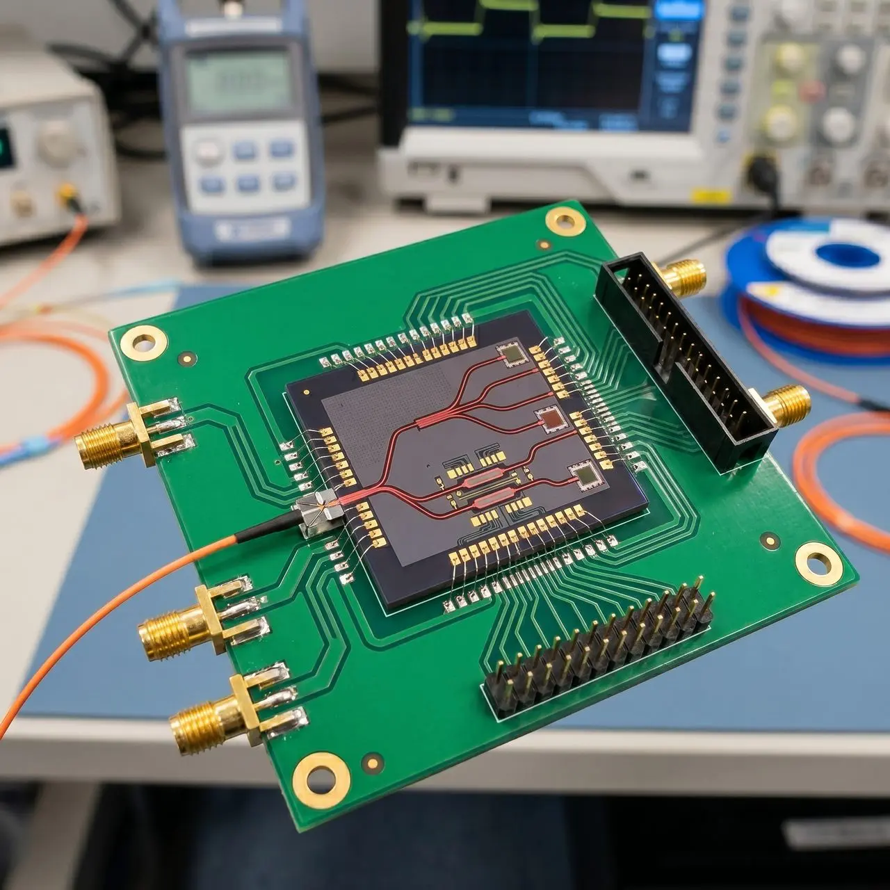
Four routes around that problem are in commercial use and none of them is free. You can mount a separate laser in the package and couple its light in, or you can bond indium phosphide dies, or whole wafers of the material, onto the silicon, or grow the material on silicon directly. The fourth option is to keep the laser well away from the heat altogether and pipe its light in down a fibre. Intel took the bonding road and says it has shipped over eight million photonic chips since 2016, carrying more than 32 million on-chip lasers between them. Ayar Labs took the opposite one, feeding its chiplets from a separate light source that can sit in a cooler part of the rack and be replaced when it dies.
The laser is a supply problem as much as a physics problem, and the money being spent on it says so more plainly than any technical paper does. Quintessent raised $40 million in a Series A in August 2026, and its own release cites a worldwide shortage of indium phosphide lasers, the light source nearly every optical interconnect depends on. The company has begun sampling a quantum dot comb laser built on gallium arsenide instead, a comb laser being one that emits many evenly spaced wavelengths at once from a single device. Sivers said in September 2026 that it is spending $30 million to expand its indium phosphide plant in Glasgow. The site is expected to be running by the fourth quarter of 2027, and only then to turn out more than 100 million continuous-wave DFB lasers a year. Those are not the investments of an industry that has solved its light source.
Each material platform is good at one thing and hopeless at another, which is why most commercial products combine two or more of them. Silicon has the fabs behind it and the transistors sitting beside it, while silicon nitride has the lowest loss of any of them and no fast modulator to go with it. Indium phosphide emits light readily and cannot be made on the 300 millimetre lines the industry is built around. Thin-film lithium niobate has the best modulators anyone has built and almost no manufacturing history behind it. The two figures usually quoted for it come from one 2018 paper, and they belong to different devices. A 20 millimetre modulator switches on 1.4 volts and answers to 45 gigahertz, while the 5 millimetre one reaches 100 gigahertz and wants 4.4 volts to do it. Bandwidth and drive voltage trade against each other, which is the thing a slide quoting both never says. Foundries are consolidating around the gap. Tower now offers silicon photonics and silicon germanium for both telecom and AI work, and its own September 2026 announcement names datacentre and telecom transceivers alongside AI cluster architectures. The research centre imec prints indium phosphide lasers onto silicon by micro-transfer printing. That technique lifts finished devices off one wafer and stamps them down on another.
One degree of warmth breaks a microring
A material’s refractive index is the measure of how strongly it bends and slows the light passing through it. Silicon’s index shifts with temperature about ten times as strongly as silica’s does, silica being the glass an optical fibre is made from. That matters most in a ring resonator, a tiny loop of waveguide that holds and releases light of one particular wavelength and gives silicon photonics much of its compactness. In a ring, a change in temperature shows up as a drift in the wavelength the ring answers to. The resonance slides along the spectrum at roughly 63 picometres per degree, a coefficient Intel measured on rings from its 300 millimetre silicon photonics line. Padmaraju and Bergman put the consequence without decoration, writing that for typical applications a deviation of more than one kelvin will render a microring device inoperable.
The remedy is to heat the ring on purpose with a small electric heater and hold it at whatever temperature keeps it in tune, and that costs both power and time. Padmaraju and Bergman’s review collects the tuning powers in one place. Conventional tuning runs at around 100 milliwatts per free spectral range, which is the span over which a ring’s response repeats itself. The best demonstration they list comes in at 42 milliwatts, and designs that lift the ring clear of the substrate beneath it reach between 2.4 and 4.9 milliwatts. Thermal phase shifters answer in one to ten microseconds and leak heat into their neighbours as they work, which is why the 2024 roadmap names them as a brake on building larger circuits. Every bit of this has to work next to a switch chip throwing off kilowatts.
The optics have moved onto the switch package
Co-packaged optics is the idea that finally pulled photonic chips out of the faceplate and set them down on the same substrate as the switch chip they serve. Broadcom got there first with Bailly, a 51.2 terabit Ethernet switch it said it had delivered to customers in March 2024, and followed it with a 102.4 terabit part in October 2025. NVIDIA announced two of its own in March 2025, Quantum-X Photonics for InfiniBand and Spectrum-X Photonics for Ethernet, of which the Ethernet part is the one the company now dates to the second half of 2026.
Read the verbs in these announcements, because they are carrying more weight than the numbers are. Broadcom’s October 2025 release opens by saying the company is now shipping the Tomahawk 6 Davisson. Further down, the same release says Broadcom is currently sampling that device to early access customers and partners, and sampling is not the same thing as shipping. NVIDIA gives the Quantum-X InfiniBand part no date at all, and the Quantum-X unit Lambda unboxed in June 2026 was an engineering sample rather than a production machine. Lumentum, which sells lasers into all of it, told investors in August 2026 that its first co-packaged orders were the first signs that optics are starting to reach in-rack connectivity. Three parties with every reason to overstate their progress are all using the language of the early stages.
Quantum-X Photonics for InfiniBand and Spectrum-X Photonics for Ethernet, announced March 2025, built with TSMC and using micro-ring modulators. NVIDIA puts a pluggable interface at often 30 watts against as little as 9 watts co-packaged. An early Quantum-X InfiniBand switch reached Lambda in June 2026 as an engineering sample, and NVIDIA dates the Spectrum-X Ethernet part to the second half of 2026.
Bailly paired eight 6.4 terabit optical engines with a Tomahawk 5 switch in March 2024, the first 51.2 terabit co-packaged Ethernet platform. The Tomahawk 6 Davisson followed in October 2025 at 102.4 terabits, with field-replaceable laser modules. Its opening line says the switch is now shipping, while its availability section says Broadcom is currently sampling the device to early access customers.
Ships the PAM4 signal processors and coherent modules found inside a large share of the transceivers sold worldwide. It completed its purchase of Celestial AI on 2 February 2026. The December 2025 announcement put the upfront consideration at about $3.25 billion, being $1.0 billion in cash and about 27.2 million shares, with up to about $2.25 billion more in contingent stock on revenue milestones. Summing the two gives a maximum near $5.5 billion, which is our arithmetic and not a figure Marvell gave. That release also says Marvell expects meaningful revenue from Celestial AI in the second half of its fiscal 2028.
Sells TeraPHY, a chiplet that gives a processor an optical port over the UCIe standard, fed by a remote multi-wavelength light source. It raised a $500 million Series E in March 2026 at a $3.75 billion valuation, with a further $150 million in September. Its own language is manufacturing-ready rather than shipping.
The Passage M1000 is a 3D photonic interposer quoting 114 terabits a second of optical bandwidth across 256 fibres, eight wavelengths apiece. Its launch on 31 March 2025 announced an interconnect product for XPUs and switches, not a computer. The analog accelerator the company was founded on no longer appears on its product pages.
A pioneer with the largest claimed volume of any single supplier. It handed its pluggable transceiver module line to Jabil in October 2023 while keeping components and optical I/O, and demonstrated a 4 terabit optical compute interconnect chiplet at 5 picojoules a bit in 2024. That chiplet remains a prototype, by the description Intel itself gave it.
Builds an interposer that assembles photonic and electronic parts at wafer level, with a hybrid laser source. Its June 2026 quarter shows about $570,000 of revenue against $796.3 million of cash and short-term investments, after a $400 million financing in May, and reports an initial $50 million order from Lumilens. POET announced on 27 April 2026 that Marvell had cancelled all the purchase orders it had received from Celestial AI. Marvell’s stated reason was that POET had disclosed Purchase Order and shipping information in contravention of its confidentiality obligations. That is a contract dispute rather than a judgment on the part. On its revenue line alone POET is a platform with a balance sheet rather than a volume supplier.
Optical computing has one named paying customer
Computing with light, rather than merely communicating with it, keeps a separate scoreboard from everything above, and that scoreboard is a thin one. The strongest published result is Lightmatter’s, in Nature in April 2025. It put six chips in a single package, photonic tensor cores beside conventional control dies, with 50 billion transistors and about a million photonic components across the six of them together. The paper’s first figure caption gives 12 nanometres for the two control dies and no node at all for the photonic ones. Neither source splits that transistor count between the six. The machine ran real networks, including ResNet and BERT, at 65.5 trillion operations a second on 78 watts of electrical power and 1.6 watts of optical power. The arithmetic is a sixteen-bit block floating-point format of the company’s own. The paper’s own claim is accuracy rather than efficiency, and that distinction matters. Near-electronic precision, meaning answers nearly as exact as an ordinary electronic chip would give, was the piece that had been missing from every earlier attempt at multiplying matrices with light.
What the company did next says more than the paper does. Lightmatter’s product line today is an interconnect rather than a computer, and the analog accelerator it was founded to build survives only as a trademark in the website footer. Q.ANT, a German firm working in thin-film lithium niobate, announced its first commercial customer in May 2026. The buyer is a hosting provider called IONOS rather than a research group, which is the more encouraging sort of customer to have. Even so, Q.ANT sells the machine as a co-processor that sits beside the graphics processors, or GPUs, that do the heavy lifting, not as a replacement for them.
Lidar is the round photonics lost
Automotive lidar, which is the laser equivalent of radar and lets a vehicle build a three-dimensional picture of the road ahead, looked for years like the second big market. The coherent version of it, meaning the kind that compares the returning light against the beam that was sent out, genuinely is a photonic chip story. Aeva builds what it calls lidar on chip, using frequency-modulated continuous wave ranging. That method sweeps the laser steadily through a range of wavelengths, so the comparison at the receiver measures a target’s velocity directly as well as its distance. The company delivered C-samples to Daimler Truck in May 2026, a late stage in the qualification ladder a car maker puts a supplier through, and it has a passenger car programme aimed at production in 2028.
The volume, however, went somewhere else entirely. Hesai shipped about 628,000 lidar units in the second quarter of 2026 alone, on revenue of 860.8 million renminbi. It did so with direct time-of-flight ranging, which times how long a pulse takes to come back rather than comparing the return against the beam that was sent. Hesai’s annual report gives time of flight as the operating principle for every product in its range. Aeva booked $6.1 million of revenue in the same three months, of which only $2.5 million was product revenue, the rest coming from professional services. One of those two companies is in volume production and it is not the photonic one.
Mobileye ended its own frequency-modulated lidar programme in September 2024, and its announcement named the reason: continued better than expected cost reductions in third-party time-of-flight units. Those are the simpler sensors that time how long a pulse takes to come back. Luminar filed for Chapter 11 on 15 December 2025, and its plan took effect on 6 April 2026. Luminar, though, used a fibre laser and discrete detectors and was never a silicon photonics company, so its collapse says rather less about the technology. Mobileye’s decision is the one that indicts it, because the crude option got cheap faster than the elegant one did.
Outside data movement the tally is short
Photonic biosensing amounts to one clear commercial instance rather than a whole field. Genalyte’s Maverick system watches for binding events, the moments when a molecule in a patient sample latches onto a matching molecule waiting on the chip. It reads them off an array of microring resonators on a disposable silicon chip, and holds FDA clearances from 2019 and again in July 2024. Having a clinical chemistry instrument cleared by a regulator is a great deal more than running a demonstration, and it is still one product.
Navigation is the other live one, and it suits the technology unusually well. ANELLO Photonics makes an optical gyroscope on a photonic chip, a device that senses rotation by sending light both ways around a loop and watching for the difference between the two paths. The company launched its Aerial inertial navigation system at CES in January 2026, offering it for evaluation with production shipments beginning in the second quarter. A gyroscope of that sort wants very low waveguide loss and no fast modulators at all, which plays to silicon nitride’s strengths rather than exposing its weaknesses.
Several applications routinely credited to photonic chips do not belong on the list at all. The waveguide combiners that place an image in front of the eye in augmented reality glasses are diffractive optics on glass, with no modulators and no detectors anywhere in them. Calling them integrated circuits is a category error rather than a quibble. The handheld near-infrared spectrometers sold into food and farming, which identify a substance from the pattern of light it absorbs, use filters and detector arrays, and the chip-scale versions of those remain laboratory results. Rockley Photonics spent years and a public listing trying to put spectroscopy on a wrist, and went through Chapter 11 in 2023.
Packaging and test cost more than the chip
Packaging an electronic chip is a matter of lining up solder bumps, which is exacting work but thoroughly understood. Packaging a photonic chip means aligning the core of an optical fibre with a waveguide to a fraction of the width of a red blood cell. That alignment then has to hold through years of heating and cooling as the machine runs and rests. Estimates repeated across the peer-reviewed literature put packaging, assembly and test at 70 to 80 per cent of what a photonic integrated circuit costs to make. The same estimates put it at about 20 per cent for an ordinary electronic one. The four studies they rest on were published between 2011 and 2022, a long window in a business whose packaging has since moved onto the switch package itself. On a photonic part the chip itself is the cheap bit, which is the reverse of the electronic case.

That cost reaches back into the design, because the way light gets onto the chip has to be settled early. An edge coupler, which meets the fibre at the polished edge of the die, gives low loss but consumes chip area and demands precise active alignment. Active alignment means nudging the two parts into place with the light switched on and the signal watched. A grating coupler lets light in through the top surface instead. It is compact, can sit anywhere on the surface, and lets you test the die while it is still in the wafer. The price is fussiness about polarisation, temperature and wavelength. Choosing between them is partly a decision about how you intend to test the thing, taken before a single waveguide has been drawn.
FormFactor sells the probe cards the industry uses to make contact with chips while they are still in the wafer, and it states the test gap in one line. Optical probing wants alignment inside a micrometre, while most electrical probers today land within tens of micrometres. That is not a matter of tuning an existing machine but of building a different class of machine altogether. Ports have generally been aligned one at a time, so test time scales with the port count rather than the die count, and the fix being pursued is aligning several sites at once. Our report on wafer-level photonic testing covers how that is being automated.
The design kits arrived twenty years late
A chip designer working in silicon leans on a mature process design kit, the bundle of rules and verified compact models a foundry supplies so a circuit can be simulated before it is built. The designer also has a real market in third-party building blocks, bought ready-made from other firms. Photonics has almost none of that. The same Nature Communications roadmap says that mature kits and the abstraction languages that let a designer work at a higher level remain at a very early stage. It adds that third-party design blocks are mostly non-existent, and that foundries wall off their best processes to protect the investment. Companies in this field therefore behave as integrated device makers, designing and building everything themselves, because the alternative does not exist yet.
The gap is closing, but in steps small enough that each one can be dated exactly. OpenLight and Tower made a design kit for an indium-phosphide-on-silicon platform available inside Cadence’s tools in August 2026. That is how recently a designer could reach a laser-integrated process from a mainstream tool, as our coverage of that design kit release described. Prototyping access tells the same story from another direction. The imec silicon photonics platform offered to European researchers is a 130 nanometre process rated at 50 gigabits a second a lane, at a time when the market ships 1.6 terabit modules.
Prototyping is at least affordable. A shared wafer run is one in which many customers’ designs travel through the factory together on a single wafer and split the bill between them. Such a run buys 20 unpackaged dies from AIM Photonics at about $36,000 for members on an 8 square millimetre active die, and about $43,000 for everyone else. A block of about five millimetres on imec’s active platform costs €44,000 through Europractice, so two institutes on two continents land in the same range. A first prototype costs tens of thousands rather than millions, and the American programme sits inside a defence manufacturing institute, as our note on AIM Photonics sets out.
The accelerator is the next step inward, and the hardest
Photonic chips are not a replacement for electronics, and the industry has largely stopped implying that they might be. They are a fix for one specific failure of electronics, the rising cost of shoving bits down a wire, and on that job they keep taking territory from copper. The optics have moved from the long-haul span to the rack, from the rack to the faceplate, and now onto the switch package itself, and each of those steps inward has taken roughly a decade.
The next step inward is the accelerator, and it is the hardest one yet because it asks the most of everything that is already difficult. It places a temperature-sensitive optical circuit, and in most designs a laser made of another material entirely, beside the hottest silicon in the building. It then asks a supply chain with immature design kits and no third-party parts market to deliver all of that at volume, and at reliability grades photonics has never had to meet. Marvell has told investors that revenue from the technology starts in the second half of its fiscal 2028. Its financial year ends in January, so that is a window closing at the start of 2028, and it is the most useful date anyone has given.
For a buyer, that turns into one plain instruction and one number. Co-packaged optics in 2026 is a sampling-stage purchase rather than a shipping one, and the suppliers say so themselves if you read their availability sections rather than their headlines. The questions worth putting to a vendor are about the laser supply and the packaging line rather than about the photonic chip, because that is where the cost and the schedule risk sit. Packaging, assembly and test are estimated at 70 to 80 per cent of what the part costs to build. The indium phosphide those lasers need is scarce enough that Sivers’ new capacity does not come on line until the fourth quarter of 2027.
The number is what waiting costs, and it is small enough to price a vendor quote against. On Evans’s figures a 102.4 terabit switch draws about 6,400 watts with today’s pluggable modules and about 4,100 with the optics on the package. The EIA’s Table 5.3, released on 26 August 2026 with data for June, puts the average American industrial price over the twelve months to June 2026 at 8.87 cents a kilowatt hour. On that meter the 2.3 kilowatts of surplus costs roughly $1,800 a year. Running the whole pluggable switch costs about $5,000 a year at the same price, so the waste is 36 per cent of its power bill. Cooling sits on top of that, and the multiplier is the site’s power usage effectiveness, the ratio of what the building draws to what the equipment draws. A site running at 2.0 pays the $1,800 twice over, and one at 1.2 pays about $2,160 in all.
That gives the decision a ceiling, and the ceiling moves with the building. Over a five-year switch life the electricity itself is worth about $9,000 before cooling. Cooling lifts that to about $11,000 at a power usage effectiveness of 1.2, and to about $18,000 at the 2.0 an older hall runs at. A vendor asking a premium above the figure for the buyer’s own site is not selling a power saving, whatever the slide says. The difference has to be justified on rack density or port count instead. Below it the saving pays for itself, and the sums are worth redoing with the site’s own tariff. Either way the part is not on sale in 2026, Marvell’s revenue window closes at the start of 2028, and the indium phosphide capacity arrives in late 2027. Supply gates delivery here, and the electricity bill decides only what the wait costs and what a premium is worth paying.
For an investor the discount is sharper still. The strongest published result in optical computing, Lightmatter’s, came from a company whose product line is now an interconnect rather than a computer. The only named commercial customer in the field is a hosting provider, IONOS, buying a Q.ANT machine sold as a co-processor beside GPUs rather than as a replacement for them. One named customer is not a market, and an optical computing position today is a research bet with a single commercial reference behind it.
Everything above concerns light used as a carrier of ordinary bits. The same waveguides, modulators and detectors can be built to manipulate single photons one at a time instead. That is a different discipline with different economics, and it is covered in our guide to how photonic quantum computers work. The classical business has revenue, customers and a supply shortage to show for itself, while the quantum one has a physics argument and a roadmap, so it is worth keeping the two firmly apart.
Frequently asked questions
What is a photonic chip?
It is an integrated circuit that carries information as light rather than as electric charge. Waveguides guide the light, modulators write data onto it, and photodetectors convert it back into current. Most photonic chips made today move data between machines instead of performing calculations.
Are photonic chips faster than electronic chips?
Not in the sense usually meant. Light in a silicon waveguide travels at about a quarter of its free-space speed, which is roughly half the speed of a signal on a printed circuit board trace. The advantage is that an optical link uses about the same energy whether it runs one centimetre or one kilometre, while an electrical link costs more the longer it gets.
Why can photonic chips not replace processors?
Three walls stop photonic chips from doing the job of a processor. There is no practical optical transistor, because optical devices generally fail the criteria for cascadable logic with gain and signal restoration, and light levels depend on loss. There is also no optical memory, only delay lines, and an optical component cannot shrink below the wavelength of the light it carries, so a photonic multiply cell takes far more area than the electronic multiply unit it would replace. Measured as work done for each square millimetre of silicon, a current electronic accelerator is around fifty times denser than the best published photonic one. That is at the 500 megahertz clock the photonic machine was measured at, and it falls to about thirteen times at its 2 gigahertz design clock. Comparing the two multiply units directly gives about seventeen times, and that comparison does not depend on the clock at all. Both die areas come from the free figure caption and the free supplementary information of the Nature paper, DOI 10.1038/s41586-025-08854-x. Energy divides the same way. On measured silicon the electronic part is ahead, at about 1.41 trillion operations a second for each watt against 0.82 at matched sixteen-bit precision. On the design clock the paper’s own Table S4 puts the photonic part ahead, at 1.75 against 1.41. Isolating only the energy the photonic core spends encoding its vectors and weights, which leaves the digital host out, the paper reports 262 trillion operations a second for each watt. Every one of these figures describes a single published device from a single paper, and no other vendor has published enough for a second machine to be compared the same way.
What are photonic chips made of?
Four platforms dominate. Silicon on insulator brings the fabs and the electronics; silicon nitride brings the lowest loss; indium phosphide is the one that can emit light; and thin-film lithium niobate makes the best high-speed modulators. Most commercial products combine at least two of these in one package.
Why does a silicon photonic chip need a separate laser?
Silicon has an indirect bandgap, so an excited electron mostly releases heat rather than a photon, and it cannot provide the optical gain a laser requires. Light has to come from a III-V material such as indium phosphide, either bonded onto the silicon, mounted in the package, or piped in from a remote source over fibre. This is the single biggest cost and supply constraint in the industry.
What is co-packaged optics?
It means putting the optical engines on the same substrate as the switch or processor chip rather than in pluggable modules at the faceplate. Putting the photonic chips on the package removes the board trace between the switch and the optics, and with it most of the signal conditioning needed to recover what that trace costs. Broadcom and NVIDIA both have products, though Broadcom describes its 102.4 terabit switch as sampling to early access customers and NVIDIA dates its Ethernet part to the second half of 2026.
Where are photonic chips actually used today?
Photonic chips ship overwhelmingly in optical transceivers for data centres and telecommunications, a market LightCounting sizes at $23.8 billion in 2025, though not every module in that total contains a photonic integrated circuit. Beyond it there is one FDA-cleared photonic biosensor, an optical gyroscope entering production, and a coherent lidar programme that has not reached volume. Chip-scale spectrometers and augmented reality combiners are usually miscredited to photonic chips.
Is optical computing real?
It is real as research and marginal as a business. Lightmatter published a working photonic processor in Nature in 2025 that ran standard neural networks at near-electronic precision, then moved its product line to interconnect. Q.ANT announced a first commercial customer in May 2026 and sells its system as a co-processor beside GPUs, not as a replacement.
Why are photonic chips expensive to make?
Because most of the cost is not in making the chip. Estimates in the literature put packaging, assembly and test at 70 to 80 per cent of the total, against about 20 per cent for an electronic chip, largely because a fibre has to be aligned to a waveguide within a fraction of a micrometre and held there. Optical wafer test needs sub-micrometre alignment where electrical probers work to tens of micrometres.
How do photonic chips relate to quantum computing?
Photonic chips of the two kinds share their components and very little else. Photonic quantum computers use the same waveguides, splitters and detectors to manipulate single photons, where classical photonic chips send billions of photons per bit. The classical business has large revenues today, while the quantum one is still proving its architecture.




See today’s quantum computing news on Quantum Zeitgeist for the latest breakthroughs in qubits, hardware, algorithms, and industry deals.