
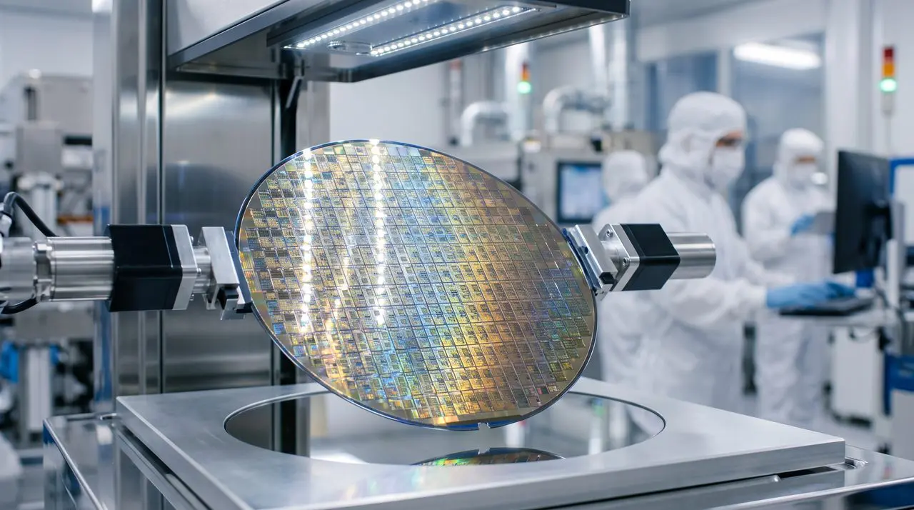
As data rates climb beyond 800G, silicon photonics is emerging as a key technology for efficiently moving massive amounts of data, yet verifying the performance of these complex devices presents significant hurdles. Manufacturers are now focused on wafer-level testing, combining traditional semiconductor probing with precision optical alignment to validate designs before packaging.
FormFactor demonstrated how automated optical alignment improved silicon photonics testing efficiency through its collaboration with IHP, addressing a critical need as the industry looks toward 1.6T optical interconnects. This testing is a crucial step in moving these increasingly complex devices from development into manufacturing.
Optical Alignment Challenges in Silicon Photonics Testing
Achieving precise alignment, often measured in microns and even sub-microns, presents a significant hurdle compared to traditional electrical wafer testing where simple contact is sufficient. Unlike electrical probing, photonic testing demands efficient light coupling into microscopic waveguides, a process acutely sensitive to even minute positional changes.
The difficulty stems from the combined electrical and optical nature of silicon photonics devices; they integrate electrical circuitry with optical components like waveguides, modulators, and detectors on a single chip, creating a unique set of measurement challenges. Engineers must not only verify device functionality and high-speed interfaces electrically, but also simultaneously characterize optical properties such as modulation efficiency and fiber coupling efficiency.
Collecting these measurements independently increases test time and introduces variability, a problem modern integrated test solutions address by coordinating both measurement environments within a single automated workflow. The company blog states that as silicon photonics moves from research into high-volume manufacturing, manual testing quickly becomes a bottleneck, emphasizing the need for speed and repeatability. Maintaining consistent measurement accuracy is paramount, as even slight vibrations, thermal expansion, or drift can alter optical coupling efficiency and yield inconsistent results.
Several factors can introduce variability during wafer probe testing, including mechanical vibration, temperature fluctuations, and probe wear. This is particularly important as the industry progresses toward 1.6T optical interconnects, demanding increasingly precise and reliable testing methodologies.
Thermal effects further complicate the process, as temperature influences modulator efficiency, detector sensitivity, and overall electrical performance. Comprehensive characterization requires evaluating devices across a wide temperature range to understand real-world operating behavior. Integrating thermal control into wafer-level testing allows engineers to maintain stable optical alignment while assessing performance under varying conditions. Successfully transitioning from research laboratory characterization to production testing demands equipment designed for these challenges.
The shift from manual processes to automated systems is not merely about speed; it’s about scalability and reducing reliance on specialized expertise. FormFactor’s Autonomous Silicon Photonics platform aims to streamline optical alignment. As silicon photonics devices become more complex, integrating automation into the probe station is becoming one of the most effective ways to improve throughput while maintaining the precision required for next-generation photonic integrated circuits, ensuring these foundational technologies can move efficiently to the fabrication facility.
Throughput Automation for High-Volume Silicon Photonics
The demand for increased data throughput is driving a fundamental shift in how silicon photonics devices are validated for manufacturing, with FormFactor addressing key bottlenecks through automation. While initial characterization of photonic integrated circuits (PICs) occurred primarily in research laboratories, the transition to high-volume production necessitates a move away from manual testing procedures. Engineers require not only the same precision as before, but also the ability to characterize significantly more devices in a reduced timeframe without compromising measurement quality.
A primary challenge lies in the need for simultaneous electrical and optical measurements, a requirement unique to silicon photonics compared to traditional semiconductor testing. Maintaining measurement repeatability presents another significant hurdle; consistent results are paramount in semiconductor manufacturing, as all production decisions rely on trustworthy data.
The TRITON system is specifically designed to address these challenges. Many silicon photonics devices initially undergo testing in research settings where manual alignment and custom scripts are common. Manufacturing, however, requires standardized workflows, automated alignment, and minimal operator intervention. FormFactor’s solutions are designed to help engineers meet these challenges by enabling faster characterization, improved repeatability, and scalable wafer-level testing for both research and production environments, ultimately ensuring that next-generation optical technologies can move efficiently and confidently to the fab.
Repeatability & Thermal Control in Wafer-Level Testing
FormFactor is addressing the critical need for consistent measurement in silicon photonics manufacturing, a challenge amplified by the move from research to high-volume production. Maintaining measurement repeatability presents a substantial hurdle, as every production decision relies on trustworthy data; engineers need confidence that measurements taken will align with those taken in the future, irrespective of personnel or location. This integrated approach is not merely about speed, but about establishing a foundation of confidence in the characterization data and improving overall measurement consistency.
The company highlights that even minor positional changes can significantly affect measurement accuracy, underscoring the need for precise control throughout the testing process. Beyond positional accuracy, thermal effects pose a significant challenge to reliable silicon photonics testing. Temperature influences nearly every aspect of photonic device performance, impacting modulator efficiency, detector sensitivity, and electrical performance.
Many applications necessitate characterization across a broad temperature range to accurately predict device behavior under real-world operating conditions. This capability is essential for ensuring devices function predictably in diverse environments. The company’s advanced probe stations combine high-precision wafer positioning, optical fiber alignment, electrical probing, temperature control, motion control, and automated measurement software into a single platform. The benefits of this approach extend beyond faster testing and improved consistency; it also allows engineering teams to scale manufacturing without relying on an increasing number of specialized photonics experts to perform every measurement manually.



See today’s quantum computing news on Quantum Zeitgeist for the latest breakthroughs in qubits, hardware, algorithms, and industry deals.