
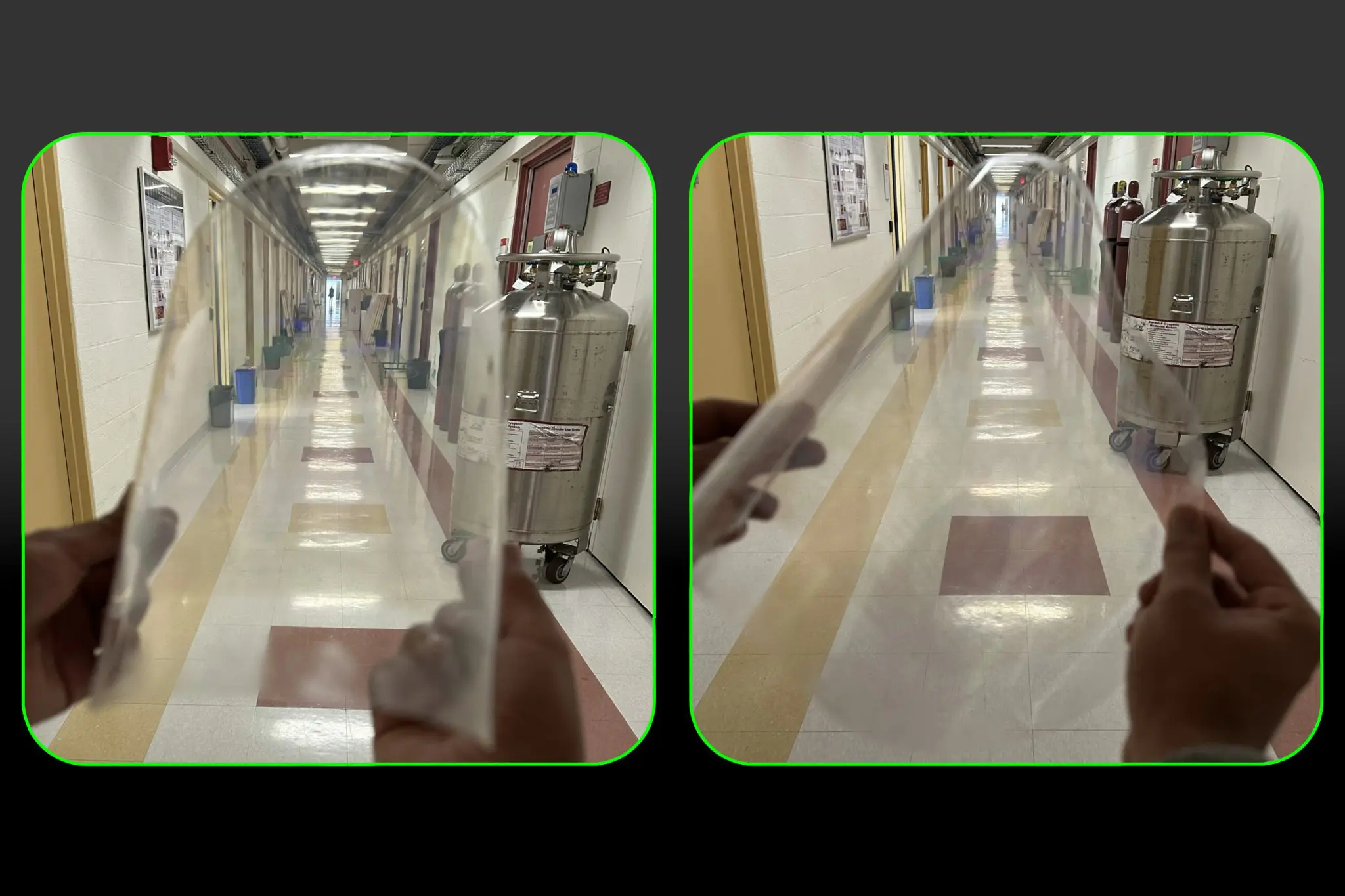
MIT scientists have developed a wafer-scale process to fabricate silicon-photonics chips that are both mechanically flexible and optically transparent, a combination previously unattainable with traditional materials. This scalable technique moves beyond limited lab demonstrations to enable mass production of advanced microchips for emerging applications.
“We’ve now developed a wafer-scale process that produces wafers that are mechanically flexible and optically transparent, enabling novel applications that weren’t previously possible with silicon photonics,” says Jelena Notaros, the Robert J. Shillman Career Development Associate Professor of Electrical Engineering and Computer Science at MIT. The new chips could lead to discreet health monitors conforming to the body and transparent augmented-reality displays for pilots.
Wafer-Scale Process Enables Flexible, Transparent Silicon Photonics
The fabrication process relies on 300-millimeter wafers, a significant increase in scale compared to previous demonstrations limited to fabricating only a few devices at a time. This wafer-scale approach, utilizing existing fabrication tools, allows for mass production and increased confidence in performance metrics, as the team can reliably produce a large number of devices meeting specifications. Achieving both mechanical flexibility and optical transparency simultaneously presented a considerable engineering challenge; traditional silicon photonics chips are rigid and opaque.
A key innovation involves a temporary support layer added during fabrication to prevent wafer shattering when flipped, a critical step in creating the flexible structure. Removing this temporary layer leaves only the oxide and waveguiding layers, resulting in a remarkably thin and transparent chip. This process, validated through experimentation, demonstrated performance exceeding the requirements for intended applications.
The team’s work confirms the viability of applications benefiting from these unique properties. Notaros envisions uses ranging from discreet health monitors that conform to the body to transparent augmented-reality displays capable of fitting the curve of a pilot’s helmet.
Because we are using s -millimeter foundry fabrication tools, we can design systems with a very large number of devices and feel confident that they are going to perform up to specifications, which is extremely important.
Tal Sneh
NY Creates Collaboration Advances 300-Millimeter Wafer Fabrication
The fabrication process now uses existing 300-millimeter foundry tools, enabling designs with a high device count and predictable performance, according to Sneh. Researchers bonded a temporary silicon wafer atop the initial rigid substrate, a critical step in managing strain during the subsequent material removal. Removing the original silicon substrate leaves a remarkably thin wafer, just a few microns thick, composed of oxide and the light-guiding layers essential for silicon photonics.
The team reports that their work expands the possibilities for silicon photonics beyond conventional rigid circuits, envisioning applications benefiting from both flexibility and transparency. They highlight the potential for novel devices. The resulting process offers a pathway to creating devices previously unattainable with standard semiconductor manufacturing.
We’ve now developed a wafer-scale process that produces wafers that are mechanically flexible and optically transparent, enabling novel applications that weren’t previously possible with silicon photonics.
Jelena Notaros
Stress Management Key to Ultrathin Wafer Production
Managing stress within the silicon itself proved central to achieving these ultrathin wafers. During fabrication, even slight bowing of the material could lead to surface ripples or catastrophic shattering on the production line, according to the team. “As we were flipping the wafers over on these substrates, if the strain isn’t properly managed and the wafer isn’t perfectly flat, it is going to get ripples across its surface or even shatter in the fabrication line,” explained Dyer.
To mitigate this, the researchers adhered to low-temperature processes, maintaining temperatures at or below 500 degrees Celsius throughout the entire procedure. Sneh detailed how a temporary silicon wafer provided important support during this delicate process. “Thanks to the fact that we added that rigid temporary support before we flipped the wafer over, we can go all the way down so we are just left with the oxide and waveguiding layers,” she said.
The team then bonded a transparent polyester film to the ultrathin layers, completing the wafer’s transformation. The ability to fabricate at the 300-millimeter scale, using existing foundry fabrication tools, is a key advancement, as it allows for high-volume production, the researchers state.
We’ve now developed a wafer-scale process that produces wafers that are mechanically flexible and optically transparent, enabling novel applications that weren’t previously possible with silicon photonics. We hope that, by working closely with our colleagues at NY Creates and using the foundry at the Albany NanoTech Complex, there’s the potential for us to make the platform accessible to other groups within our research community and open these new application areas to the field of silicon photonics as a whole.
Jelena Notaros, the Robert J. Shillman Career Development Associate Professor of Electrical Engineering and Computer Science (EECS) at MIT, a member of the Research Laboratory of Electronics, and senior author of a paper on this fabrication platform
Performance Validated: Waveguiding, Bendability, and Optical Transparency
Waveguiding performance remained consistent even after repeated mechanical stress, demonstrating the robustness of the newly developed wafers. Researchers tested chips containing integrated waveguides of varying lengths to quantify their ability to channel light, confirming expected waveguiding properties throughout the fabrication process. Further validation involved bending a chip thousands of times around cylinders of differing diameters; performance showed no degradation when bent around a cylinder comparable in size to a small screw.
The platform’s resilience was pushed further, with noticeable performance decline only occurring after multiple bends around a toothpick, a diameter significantly smaller than anticipated for most applications. “This experiment validated that the platform can be used for our proposed applications, performing even well beyond the metrics required for these intended systems,” stated Garcia Coleto, highlighting the wafers’ suitability for demanding environments.
These results confirm the feasibility of integrating the chips into applications like augmented-reality displays, potentially replacing bulky optical systems currently used in pilot visors. The team is now focused on incorporating more complex components and refining the design to enhance both waveguide efficiency and transparency. They envision a future where these flexible, transparent chips enable a range of new technologies, benefiting areas from discreet health monitoring to advanced augmented-reality interfaces.
We realized that there are a lot of applications that would benefit from having a chip that is flexible and transparent.
Jelena Notaros, the Robert J




See today’s quantum computing news on Quantum Zeitgeist for the latest breakthroughs in qubits, hardware, algorithms, and industry deals.