
Arrays of low-quality cavities precisely aligned with silicon T centres enable faster measurements of these quantum systems, removing a key limitation hindering thorough statistical analysis of their properties. This approach yields a six-and-a-half times increase in signal strength, translating into a fortytwofold speedup compared to previous methods relying on individually tuned high-quality cavities. A new method for studying defects within silicon materials, called “T centres”, could be important for developing quantum technologies.
An array of tiny structures called cavities amplifies light emitted by T centres, speeding up measurements fortytwofold without needing individual adjustments for each one; this allows accurate measurement of the number of T centres existing in a material and easier investigation of their properties for potential use in photonics and integrated circuits. Researchers at Delft University of Technology have developed a new technique to study defects called “T centres” within silicon, holding promise for future quantum technologies.
This is achieved using acoustic design principles, just like how a concert hall’s shape affects sound reverberation, measured as its quality factor, the cavity shapes control how well they trap and enhance light. By analysing statistics from this array, the team determined the density of T centres in their sample, offering an important step towards building scalable quantum devices.
Detuned cavity arrays enable rapid and calibrated silicon T centre density mapping
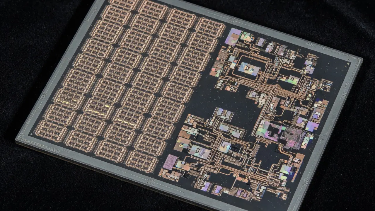
A fortytwofold speedup in measurement was achieved, a substantial improvement over previous techniques limited to individual cavity tuning for silicon T centres, quantum systems with potential applications in photonics and integrated circuits. This breakthrough stems from fabricating an array of four hundred low-quality optical cavities deliberately detuned less than 1.1 nm from the target emission wavelength; this eliminated painstaking alignment procedures previously required when using high-Q alternatives.
Statistical data gathered across these structures directly determined a density of 4.2+1.3-0.8~mathrmμm-2 of T centres within their sample without needing calibration based on external collection efficiency estimates, direct measurement had been impossible due to signal limitations.
The 400-cavity array enabled a median signal increase of $6.5× for silicon T centres, which in turn drove the fortytwofold speedup in measurement reported earlier. Fabrication at a wavelength of Λ = 520nm yielded an average cavity quality factor of 298 pm $78, with detuning averaging $0.0 pm $1.1 nm from the target emission; this demonstrates precise control despite utilising deliberately lower Q factors to avoid individual tuning requirements. Spatial variations within the fabricated array were revealed through analysis, cavities on the edges exhibited redshifted resonance wavelengths compared to those centrally located, indicating potential refinements remain in lithography’s proximity effect correction during fabrication.
Faster Defect Analysis Needs Validation Across Silicon Variants
These new broadband cavities offer substantial gains in measurement speed and direct determination of T centre density, but their applicability beyond this specific sample remains an open question; researchers acknowledge that material composition or fabrication processes could affect performance. The team successfully compared measurements against Monte Carlo simulations, computational modelling used to predict outcomes, yet extending this technique requires validating its strong performance across diverse silicon structures. Acknowledging possible shifts with differing materials or manufacturing techniques does not diminish the advance; it simply highlights a key area for future refinement.
Forty times faster measurements alongside direct assessment of defect concentration have been demonstrated within these important silicon structures. Deliberately mismatched from target wavelengths during fabrication, an array of low-quality optical cavities allowed the Delft University of Technology team to achieve fortytwofold faster measurements of silicon T centres, these defects hold promise for quantum technologies due to their compatibility with existing infrastructure. This approach enabled direct determination of T centre density in their sample at 4.2+1.3-0.8~mathrmμm-2, without relying on estimates of light captured by the measurement apparatus; this had long hindered accurate analysis.
This research demonstrates a method for increasing photon emission from T centres in silicon using an array of 400 confocally-addressable low-Q cavities detuned by less than 1.1nm. The technique yielded a median signal increase of 6.5 times, resulting in a fortytwofold speedup for measurements, a benefit because weak emissions previously slowed data collection. By comparing results to Monte Carlo simulations, researchers directly determined a T centre density of 4.2+1.3-0.8~mathrmμm-2 without needing to estimate light capture efficiency; this offers new possibilities for characterizing these quantum materials.
👉 More information
🗞 Large-scale characterisation of silicon T centres with tuning-free broadband cavities
✍️ Christian F. Primavera, Matteo Pirro, Elena Volkova, Joan Mascaró Rosselló, Cas C. P. E. Hoppenbrouwers, Bram Zijlstra, Ronald Hanson and Carlos Errando-Herranz (Delft University of Technology)
🧠 ArXiv: https://arxiv.org/abs/2611.15412

See today’s quantum computing news on Quantum Zeitgeist for the latest breakthroughs in qubits, hardware, algorithms, and industry deals.