
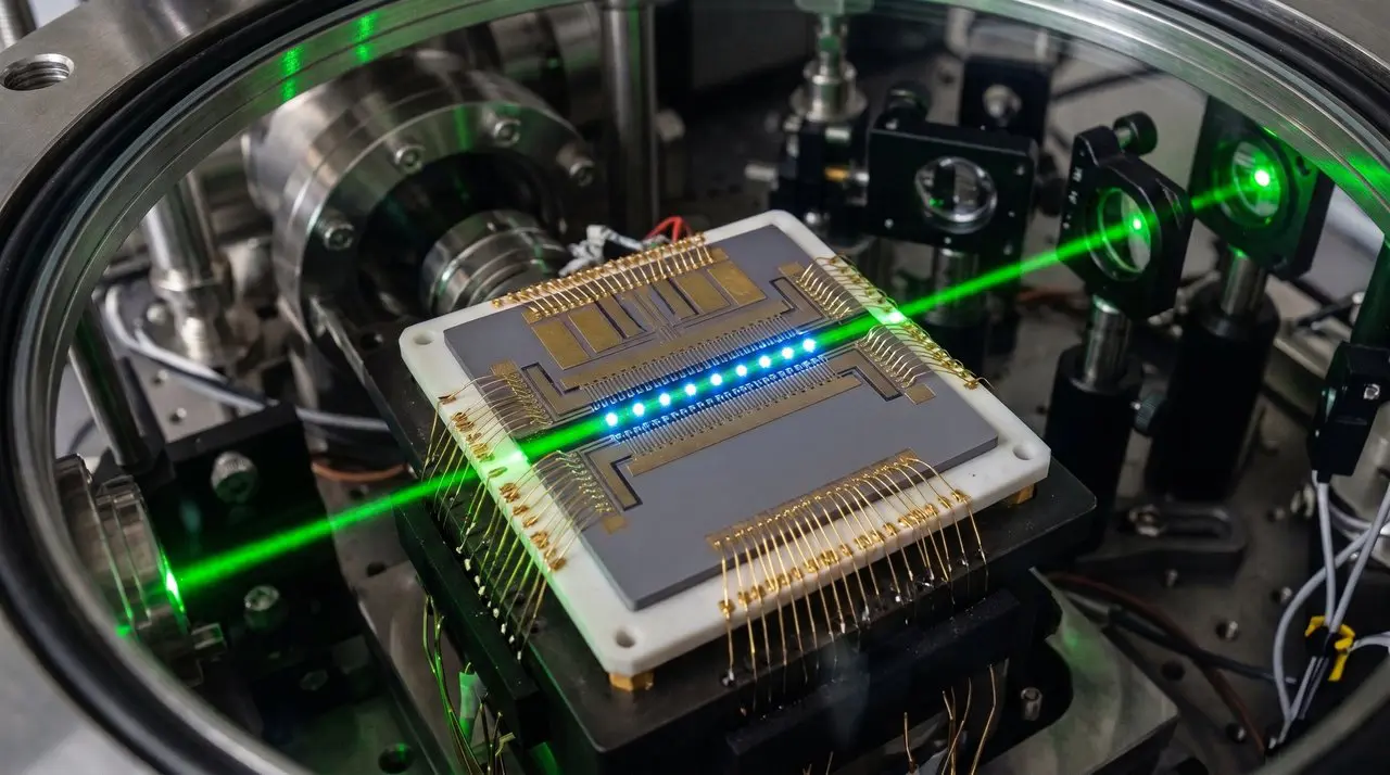
Integrating high-performance blue light sources onto silicon nitride photonic circuits previously presented key hurdles due to limitations in existing bonding techniques. Micro-transfer printed blue lasers have now been realised on a silicon nitride platform, overcoming challenges associated with releasing devices from their original substrate via optimised electrochemical etching. The technique efficiently integrates blue lasers onto silicon nitride chips by moving tiny light sources from their original substrate onto a new platform.
This advancement addresses longstanding difficulties in combining gallium nitride laser components with existing chip technology, enabling more complex optical systems. Establishing this method expands opportunities within visible light photonics for applications including medical diagnostics and virtual reality technologies. Researchers at Ghent University achieved a breakthrough in visible light photonics by integrating blue lasers onto silicon nitride chips using micro-transfer printing; the technique is akin to precisely cutting out stickers from a sheet and applying them to another surface, enabling the movement of tiny devices without damage.
Silicon nitride offers a strong platform for building optical circuits but lacks the ability to generate light itself, necessitating integration with light emitting materials such as gallium nitride, a material known for its hardness and brilliance when used to create efficient blue lasers. The team overcame longstanding difficulties associated with transferring these delicate components by optimising an electrochemical etching process that carefully releases the laser structures from their original substrate. Polish Academy of Sciences collaborated on this work.
High current density laser transfer printing unlocks scalable photonic integration
Professor Dries Van Thourhout’s team and collaborators at Polish Academy of Sciences achieved current densities exceeding 20 kA/cm². This represents an improvement over previous methods hampered by sequential processing speed in flip-chip bonding or throughput constraints associated with wafer bonding. The breakthrough enables high-density placement alongside individual pre-testing, previously impossible for large area techniques, facilitating the scalable integration of blue lasers onto silicon nitride platforms. Butt-coupled devices resulting from this process demonstrate lasing at 455nm, expanding visible light photonics for applications including flow cytometry, quantum computing, optical communications and augmented reality technologies.
Using a heavily doped sacrificial layer, successful transfer printing of blue lasers emitting light at 455nm onto silicon nitride demonstrated smooth release from bulk gallium nitride substrates. Electrochemical etching improved upon methods that compromise material quality; the team employed optimised conditions for device lift-off and placement. Coupling these transferred devices to SiN fork-shaped edge couplers achieved current densities exceeding 20 kA/cm², surpassing previous limitations. Analysis confirmed efficient light extraction with minimal optical loss during the transfer process, though long-term reliability data under continuous operation is still needed before widespread commercial viability can be fully assessed.
Gallium Nitride Laser Integration via Precision
Micro-transfer printing successfully integrated components in a manner akin to precisely cutting stickers from a sheet and applying them to another surface. This technique circumvents limitations inherent in traditional methods like full-wafer bonding or flip-chip bonding by allowing for high-density placement of individual components without precise alignment across large areas; it also permits pre-testing each device prior to application.
Adapting this approach for gallium nitride demanded new strategies due to its chemical inertness, as the strong material creates efficient blue lasers, similar to how diamonds are known for their hardness but applied here to generate specific colours of light. Gallium nitride lasers emitting at 455nm were successfully coupled to SiN waveguides after integration onto silicon nitride platforms achieving current densities exceeding 20 kA/cm².
Traditional techniques such as full-wafer bonding and flip-chip bonding present challenges with thermal mismatch or processing speed, making dense placement alongside individual device testing before integration difficult. Electrochemical etching released devices from bulk GaN substrates; it offers a viable alternative.
Gallium nitride laser integration advances compact photonics on silicon nitride
The successful integration of gallium nitride lasers onto silicon nitride provides a pathway towards smaller, more efficient devices for applications ranging from medical diagnostics to virtual reality systems. While demonstrating functional gallium nitride lasers integrated onto silicon nitride is a key step forward establishing a framework for multi-wavelength integration, scaling the process beyond initial demonstrations remains an open question. Professor Van Thourhout’s team acknowledge that vital factors like long-term device stability under continuous operation haven’t yet been fully addressed.
This advance unlocks potential across diverse fields including medical diagnostics and augmented reality systems offering brighter prospects for compact optical technologies. The team overcame significant material challenges in releasing these light sources via micro-transfer printing, paving the way for increasingly complex photonic circuits. This achievement bypasses limitations found in traditional bonding methods like full-wafer processing or flip-chip assembly which struggle with material stress or slow production speeds.
The researchers successfully integrated gallium nitride lasers on to a silicon nitride platform via micro-transfer printing. This demonstrates an alternative method to conventional integration techniques that avoids issues related to thermal mismatch or slower processing times, enabling denser device placement. The technique releases the light sources from their original substrate without compromising material quality, allowing for efficient butt-coupling to silicon nitride edge couplers. Professor Van Thourhout’s team note further work is needed to assess long-term stability under continuous operation; however, this process offers potential benefits for applications including medical diagnostics and augmented reality systems.
👉 More information
🗞 Micro-transfer Printed Blue InGaN Lasers on Silicon Nitride Photonic Integrated Circuits
✍️ Konstantinos Akritidis, Krzysztof Gibasiewicz, Han Wang, Iryna Levchenko, Max Kiewiet, Maximilien Billet, Mikołaj Chlipała, Karolina Peret-Malessa, Pol Van Dorpe, Henryk Turski and Bart Kuyken
🧠 ArXiv: https://arxiv.org/abs/2609.15390

See today’s quantum computing news on Quantum Zeitgeist for the latest breakthroughs in qubits, hardware, algorithms, and industry deals.