

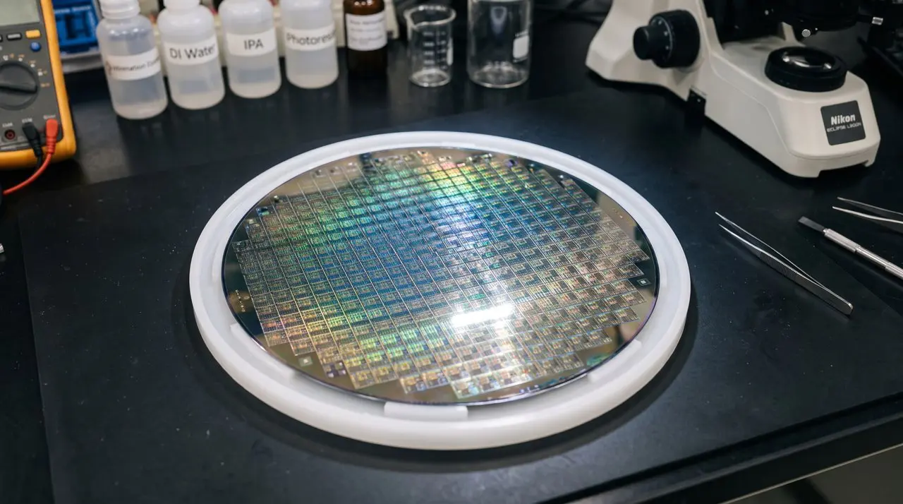
Published on July 8 in Nature Materials, researchers led by Professor REN Wencai from the Institute of Metal Research of the Chinese Academy of Sciences report achieving wafer-scale growth of monolayer MoSi₂N₄ single crystals. This high-performance p-type two-dimensional semiconductor surpasses MoS₂ in key properties like carrier mobility, thermal conductivity, and fracture strength, despite a comparable bandgap.
Until now, only polycrystalline versions of MoSi₂N₄ existed, limiting performance because grain boundaries degraded electrical transport; the team overcame this by utilizing a specialized chemical vapor deposition approach. This work establishes a promising platform for future integrated circuits and offers a general strategy for growing other 2D materials.
Cu(111) Substrate Enables Wafer-Scale MoSi₂N₄ Single-Crystal Growth
The team first created MoSi₂N₄ in 2020 by introducing silicon into a molybdenum nitride system, establishing the MA₂Z₄ family of materials, but achieving single-crystal growth remained a significant hurdle. To overcome this challenge, Professor REN Wencai’s group employed a chemical vapor deposition approach utilizing Cu(111) single crystals enriched with molybdenum and silicon atoms as the growth substrate.
They discovered that the <110> steps present on the Cu(111) surface actively promote oriented nucleation of MoSi₂N₄ domains, aligning them in a single orientation and allowing them to merge into a continuous, single-crystal film. This method is also versatile; the researchers successfully grew monolayer WSi₂N₄ single crystals on a wafer scale using the same technique.
The resulting MoSi₂N₄ exhibits an intrinsic carrier mobility of 154 square centimeters per volt-second, a value exceeding that of the commonly used semiconductor MoS₂. The material also surpasses MoS₂ in thermal conductivity, Young’s modulus, and fracture strength, while maintaining a comparable bandgap. Field-effect transistor arrays fabricated from this material demonstrated an on/off ratio of approximately 3.8 ± 1.4 × 10⁶ and an on-state current density reaching 17.96 microamperes per micrometer at a channel length of 1 micrometer, alongside improved stability compared to devices based on monolayer WSe₂.


See today’s quantum computing news on Quantum Zeitgeist for the latest breakthroughs in qubits, hardware, algorithms, and industry deals.