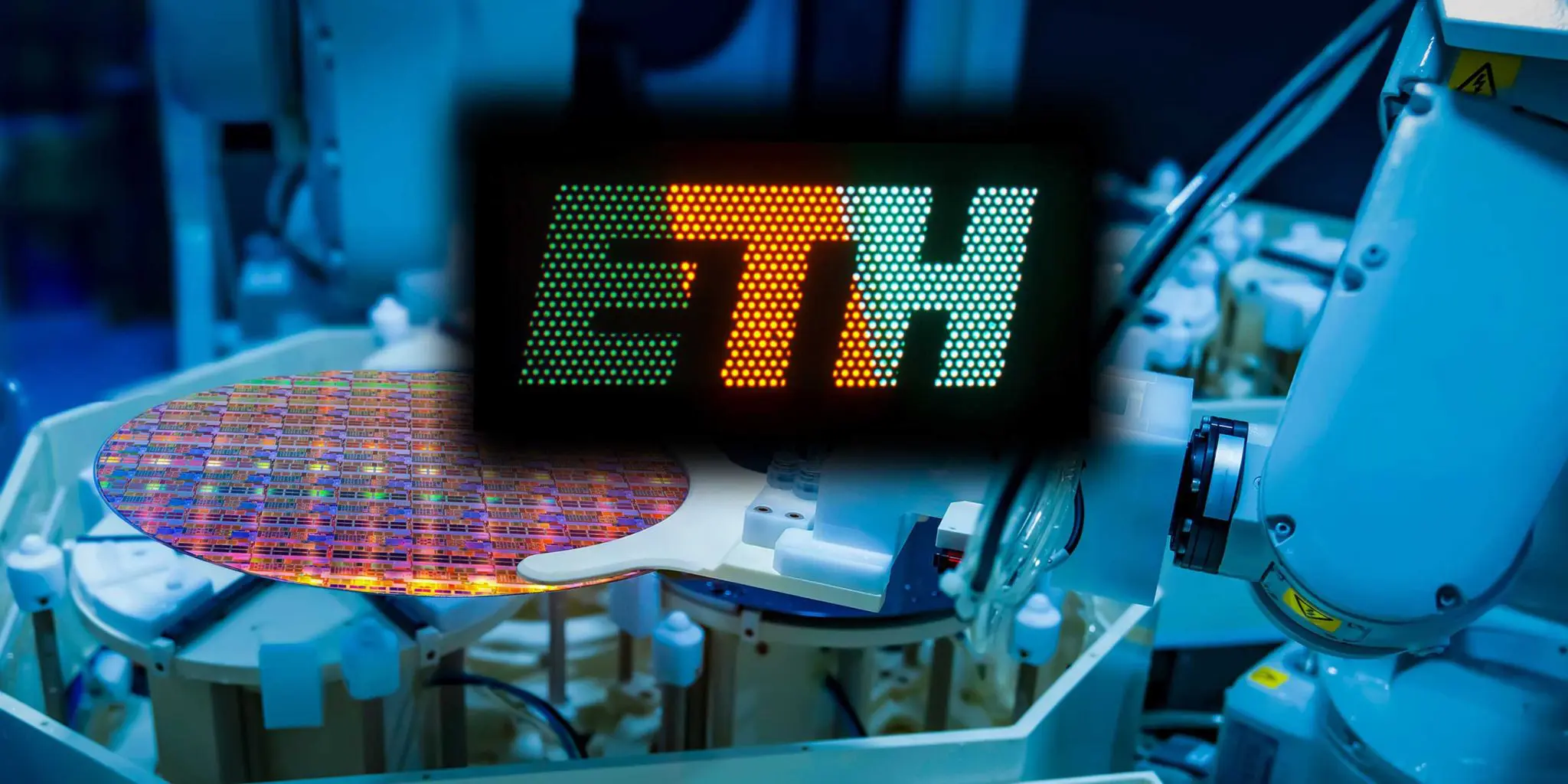
Researchers at ETH Zurich have devised a method to fabricate OLED pixels using photolithography, a process already commonplace in chip manufacturing. This breakthrough addresses a key limitation of shrinking display technology; conventional LEDs dim as they miniaturize, while these carbon-based OLEDs maintain brightness at screen diagonals less than one centimetre, ideal for augmented reality glasses and camera viewfinders.
The team created a 350 pixel array, with light-emitting polymers that function as photoresists, withstanding the harsh chemicals used in semiconductor production, as described in their recent publication in Nature. “We’ve developed a new class of long-chain molecules that can be manufactured into OLED pixels using direct light exposure,” says Yinyin Bao, formerly of ETH Zurich and now a professor at the University of Helsinki, who co-led the research with ETH Professor Chih-Jen Shih.
Luminescent Polymers Function as Photoresists in Lithography
The protective arrangement of molecular components within these new polymers is critical to their function as photoresists. Researchers successfully shielded light-emitting molecules from the harsh chemicals inherent in photolithography by spatially separating reactive and luminescent elements. This separation, achieved through a star-shaped molecular architecture, allows for cross-linking during lithography without significantly damaging the core light-emitting component, as explained by a researcher involved in the study.
“The light-emitting molecule is protected inside, whilst the reactive cross-linking groups are on the outside. This allows the photoresist to react during lithography without causing significant damage to the light-emitting core,” they stated. This approach overcomes a major hurdle in OLED manufacturing, previously incompatible with standard semiconductor fabrication processes, by using photolithography, a well-established technique for patterning materials in chip production. The team also demonstrated the university’s ability to map electromagnetic fields on chips using trapped ions, reported on July 2, 2026.
The resulting polymers, capable of withstanding the aggressive solvents used in lithography, enable the creation of fine-scale geometric structures essential for high-resolution displays. The team demonstrated the precision of this method by fabricating a 300 by 430 micrometer image of a macaw parrot, composed of 250 pixels, showcasing the potential for creating multicolour displays on an extremely small scale.
While this initial image relies on external light to excite the pixels, rather than electrical activation, it proves the feasibility of generating light with high precision exactly where it is needed, according to the researchers. They describe the spatial separation of functions as key to the success of this new class of materials, stating, “We separate the two functions spatially.”
We can use this to generate light on a small scale and with high precision exactly where it is needed.
Chih-Jen Shih, ETH Professor
Core-Shell Molecular Complex Protects OLED Pixel Integrity
Relying on a precise separation of functions at the molecular level, a design choice critical to withstanding the lithographic process, the core-shell architecture enables these new OLED pixels. Researchers achieved this by encapsulating the light-emitting molecule within a protective shell constructed from cross-linking groups, shielding it from the harsh solvents used in standard semiconductor fabrication. This innovative approach allows for high-resolution patterning without compromising the integrity of the light source itself, a feat previously unattainable with organic LEDs.
Upon exposure to ultraviolet light, the external cross-linking groups polymerize, forming a stable network that defines the individual pixel boundaries. The resulting polymer network, detailed in the team’s Nature publication, allows for the creation of 350 pixels, demonstrating the precision achievable with this method.
This collaboration, part of a decade-long initiative focused on AI and quantum computing, complements ETH Zurich’s internal research into superconducting qubits and error correction. Recent work, reported on July 2, 2026, demonstrates the university’s ability to map electromagnetic fields on chips using trapped ions, a technique potentially applicable to refining OLED manufacturing processes.
The team’s success in creating a functioning, albeit externally illuminated, 1 by 2.4 millimetre OLED logo, developed in collaboration with Hua Wang’s group, underscores the potential for scaling this technology towards applications in augmented reality and miniature displays, targeting screen diagonals of less than one centimetre.
We separate the two functions spatially.
Chih-Jen Shih, ETH Professor
High-Resolution Multicolour Image Demonstrates Photolithography Precision
The researchers produced an image of a macaw parrot measuring 300 by 430 micrometres and consisting of 250 pixels. A 1 by 2.4 millimetre OLED logo of ETH Zurich, developed in collaboration with Hua Wang’s group, also confirms the ability to produce electrically powered light-emitting diodes through this process. While currently a static image reliant on external excitation for fluorescence, the parrot serves as proof-of-concept for the technology’s potential in dynamic displays.
This demonstration is significant because it bridges the gap between fluorescent imaging and active displays, suggesting a pathway towards miniaturized screens for applications demanding high pixel density. The team’s success in integrating organic materials with established semiconductor fabrication techniques addresses a long-standing incompatibility, opening possibilities for streamlined manufacturing.



See today’s quantum computing news on Quantum Zeitgeist for the latest breakthroughs in qubits, hardware, algorithms, and industry deals.