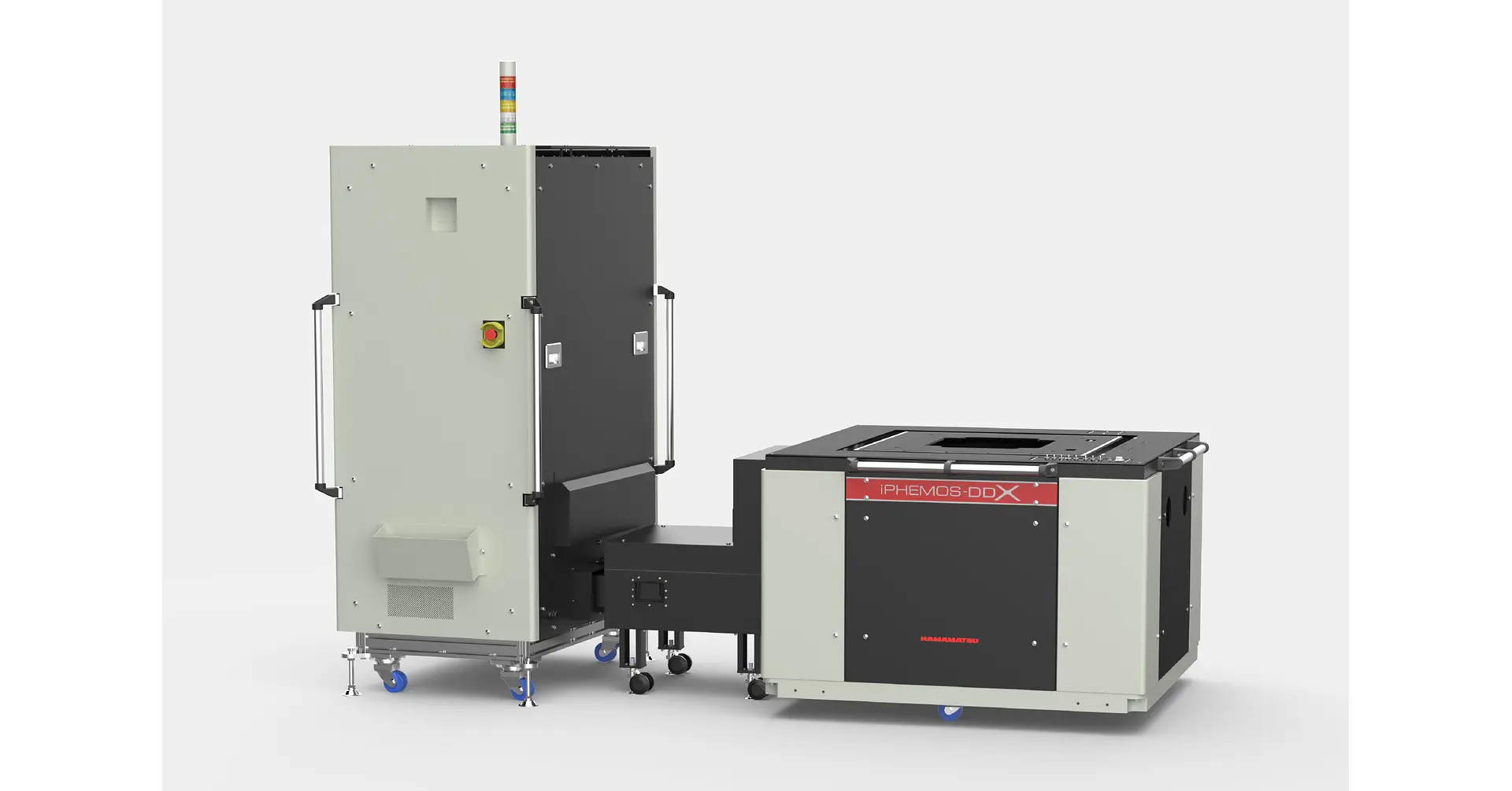
Hamamatsu Photonics is streamlining the hunt for defects in increasingly complex AI chips with the iPHEMOS-DDX, a new inverted emission microscope. The system consolidates seven distinct analysis techniques, PEM, Thermal/LIT, LSM, OBIRCH, DALS, EOP/EOFM and TD Imaging, into one platform, aiming to accelerate failure analysis workflows. Hamamatsu designed the iPHEMOS-DDX for flexible integration, enabling direct docking to existing testers from three directions. The company will publicly debut the iPHEMOS-DDX at ISTFA 2026, held in San Antonio, Texas, from October 4 through October 8.
iPHEMOS-DDX Microscope Targets AI Chiplet & 3D Package Failure
The iPHEMOS-DDX microscope supports direct docking to existing testers via connections in three directions, a feature designed to minimize disruption during integration into current workflows. This flexibility addresses a key challenge in advanced semiconductor failure analysis, where rapid setup and compatibility with existing equipment are paramount. Hamamatsu Photonics developed the system to analyze increasingly complex packages, including AI chiplets and High Bandwidth Memory, where identifying failure locations is becoming significantly more difficult.
According to Hamamatsu, this integration is a direct response to the demands of generative AI’s growth, which is driving both performance gains and structural complexity in AI chips. In 2024, Hamamatsu acquired NKT Photonics, renaming it Hamamatsu Photonics A/S in June 2026 to serve as its laser and fiber business unit. NEDO selected Hamamatsu in 2025, awarding approximately 3 billion yen over three years to Hamamatsu, AIST and RIKEN for ultra-fast camera and spatial light modulator development for neutral-atom quantum computers.



See today’s quantum computing news on Quantum Zeitgeist for the latest breakthroughs in qubits, hardware, algorithms, and industry deals.