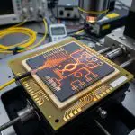
Nanoscale lensing using light scattered from single nanostructures efficiently routes photons and localizes fields on a chip. An optical waveguide and individual atoms sample near-field intensity through fluorescence; it is a non-destructive method for characterising focused optical fields. The technique enhances single atom detection efficiency fourfold, establishing these structures as platforms for trapping and manipulating atoms within hybrid photonic-atomic systems.
A new technique manipulates light at an incredibly small scale using structures built directly onto chips. Detection efficiency improved fourfold by utilising these focused fields, enabling greater control over individual atoms.
Consequently, more complex systems integrating both light and matter are now possible, with potential benefits for quantum computing and advanced sensing technologies. Researchers at the University of Science and Technology of China have developed a method for focusing light on an incredibly small scale using structures built directly onto microchips; this nanoscale lensing acts much like a magnifying glass for light, bending it to create intensely focused spots.
An optical waveguide guides photons along defined paths within these chips, enabling precise control over individual atoms. The team utilised single atoms as sensitive probes to measure these tightly-focused fields, achieving a fourfold improvement in detection efficiency through enhanced atom-photon coupling, envisioning this interaction as two dancers needing to coordinate their movements effectively. This breakthrough establishes new possibilities for building complex systems integrating both light and matter but raises the question of how readily such techniques can be scaled up for practical quantum technologies.
Enhanced single-atom detection via near-field intensity mapping confirms nanoscale optical confinement
Single atom detection efficiency increased fourfold by implementing a new near-field intensity sampling method; it overcomes previous limitations restricting sensitive measurements of nanoscale optical fields without disturbing atomic systems. This advance enables the mapping of focused light intensities at resolutions previously unattainable, opening avenues for precise control over individual atoms and their interactions with photons. The technique establishes on-chip nanostructures as flexible platforms capable of directing photons and strengthening these important atom-photon couplings, ultimately promising breakthroughs in quantum technologies such as advanced sensing and computation.
Statistical analysis verified nanoscale lensing through examination of atomic density. Specifically, changes in fluorescence collection were observed when atoms moved relative to an on-chip waveguide structure using an ‘optical conveyor belt’. We quantified this via a ‘counts ratio, measuring cumulative spatial distribution of collected photons; this revealed that modulation by the nanostructure caused a faster decrease in counts as atom position shifted, indicating stronger focusing than standard Gaussian beams.
Fitting data to a Gaussian beam profile yielded a Rayleigh length of 6.76 ±10.48μm without the lens and 17.97±2.32μm with it; however, discrepancies arose comparing fitted waist positions against numerical simulations suggesting further refinement is needed for full characterisation of this effect. An optical waveguide functions similarly to a microscopic fibre optic cable, guiding photons along defined paths on the chip surface ensuring precise control over where they interact with atoms.
The team fabricated gallium nitride waveguides measuring 200nm thick and 700nm wide on sapphire chips creating nanoscale lenses capable of manipulating light at tiny scales. Cold rubidium-87 atoms were then prepared using magneto-optic traps positioned approximately 550μm from the chip surface before transporting them via an optical conveyor belt consisting of two counter-propagating Gaussian beams with a waist around 11μm.
Directing light at the atomic scale presents challenges for scalable quantum technologies
This demonstration offers a pathway towards more compact quantum devices; however, realising practical applications hinges on overcoming limitations inherent in scaling up these systems. Successful single atom manipulation does not indicate how consistently performance would hold across multiple nanostructures integrated onto a chip, a key detail when building complex circuits. Maintaining consistent performance during scale-up remains valid as reliable functionality demands many components within such circuits.
The capability unlocks new avenues for trapping individual atoms and creating hybrid systems with significant potential in future quantum technologies despite current limitations. This new approach surpasses previous requirements of either complex fabrication or sacrificing measurement sensitivity while probing nanoscale optical fields, offering a non-destructive method to characterise tightly focussed light. The demonstration establishes on-chip nanostructures as functional components controlling both light and its interaction with single atoms; this moves beyond observation towards actively shaping these interactions. By utilising gallium nitride waveguides, microscopic structures guiding photons across the chip, enhanced atom trapping was achieved through focused near-field effects without disrupting atomic states.
The research demonstrated that nanoscale lenses fabricated from gallium nitride can focus light and enhance detection efficiency for single rubidium-87 atoms by fourfold. This is important because it provides a new way to control light at very small scales without damaging sensitive quantum systems like individual atoms. Researchers verified this effect using an optical waveguide on sapphire chips, employing fluorescence as a non-destructive method of characterising focussed fields. The authors suggest this work establishes these nanostructures as platforms capable of routing photons, localising fields, and enhancing atom-photon coupling.
👉 More information
🗞 Lensing and enhanced single atom detection via a single-pixel nanostructure
✍️ Ling-Xiao Wang, Lei Xu, Ai-Ping Liu, Guang-Jie Chen, Yuan-Hao Yang, Jia-Qi Wang, Xin-Biao Xu, Guang-Can Guo, Chang-Ling Zou and Guo-Yong Xiang
🧠 ArXiv: https://arxiv.org/abs/2608.20032




See today’s quantum computing news on Quantum Zeitgeist for the latest breakthroughs in qubits, hardware, algorithms, and industry deals.