EeroQ reports demonstrating electron transport across its “Wonder Lake” chip with high fidelity, achieving collective electron travel of tens of kilometers without detectable charge loss. The company’s research, now published in Physical Review Applied, details a selective two-dimensional shuttling system built on superfluid helium using a standard 130-nm CMOS fabrication process, requiring only 14 control lines to address 128 channels. This architecture enables all-to-all connectivity between qubits, a crucial metric for scaling future quantum computing systems. “Publication in Physical Review Applied means these results have stood up to rigorous, independent scrutiny by experts in the field,” said Nick Farina, CEO of EeroQ. “We can move electrons around a chip billions of times, over distances of kilometers in aggregate, and not lose a single one.”
CMOS Control Platform Enables Selective Electron Shuttling
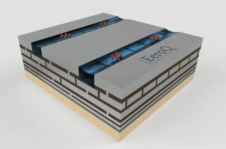
The ability to move electrons across a chip for tens of kilometers without losing a single charge particle represents a significant leap forward in qubit fidelity, as demonstrated by EeroQ’s recent publication in Physical Review Applied. This peer-reviewed validation confirms earlier announcements from the company regarding selective two-dimensional electron shuttling on superfluid helium, a process enabled by a control platform fabricated using a standard 130-nm CMOS process at SkyWater Technology. The architecture’s efficiency stems from the atomically smooth surface of liquid helium, minimizing impurities and charge traps that plague solid-state materials and typically degrade signal integrity over distance. EeroQ’s experiments utilized a network of helium-filled microchannels to clock electron packets, averaging a single electron, through a two-dimensional array.
The control architecture is remarkably streamlined, requiring only 14 control lines to selectively shuttle electrons through 128 independently addressable channels; this allows for precise routing between storage sites, on-chip sensors, and designated gate zones. The scale of electron transport achieved is particularly noteworthy, with the collective distance traveled by electrons during testing reaching tens of kilometers, which underscores the potential for building large, highly connected quantum systems. EeroQ, founded in 2017, believes this CMOS-compatible approach to quantum computing offers a pathway to rapid scalability, leveraging existing semiconductor manufacturing infrastructure to reduce resource demands and accelerate development.
We can move electrons around a chip billions of times, over distances of kilometers in aggregate, and not lose a single one.
Nick Farina, CEO of EeroQ
Lossless Electron Transport Achieved on Liquid Helium
The pursuit of stable qubits remains a central challenge in quantum computing, with current systems often hampered by signal degradation and decoherence. Solid-state qubits, while promising, frequently suffer from impurities and charge traps that limit fidelity and scalability. EeroQ is addressing these limitations with a novel architecture utilizing electrons traveling on superfluid helium, and recent validation of their findings in Physical Review Applied confirms the potential of this approach. The team reports that electrons were shuttled across the chip for a collective distance exceeding tens of kilometers without any detectable charge loss, a feat enabled by the atomically smooth and exceptionally pure surface of liquid helium. This lossless transport is achieved through a network of helium-filled microchannels, analogous to the charge-coupled devices found in digital imaging, but with a significantly reduced error rate.
This selective two-dimensional shuttling allows for the creation of packets containing, on average, a single electron, and precise movement between storage sites, sensors, and designated locations on the chip. As Nick Farina stated, that kind of lossless transport is exactly what you want from a mobile qubit, the type future quantum computers will be built upon. The ability to achieve all-to-all connectivity between qubits, facilitated by this architecture, is particularly significant for implementing advanced quantum error correction schemes, paving the way for more robust and scalable quantum processors.
Using just 14 control lines, the team selectively shuttled electrons through any of 128 independently addressable channels, moving them between storage sites and on-chip sensors and bringing packets together at chosen locations.
Source: https://eeroq.com/eeroq-electron-shuttling-achievements-published-in-physical-review-applied/




See today’s quantum computing news on Quantum Zeitgeist for the latest breakthroughs in qubits, hardware, algorithms, and industry deals.