

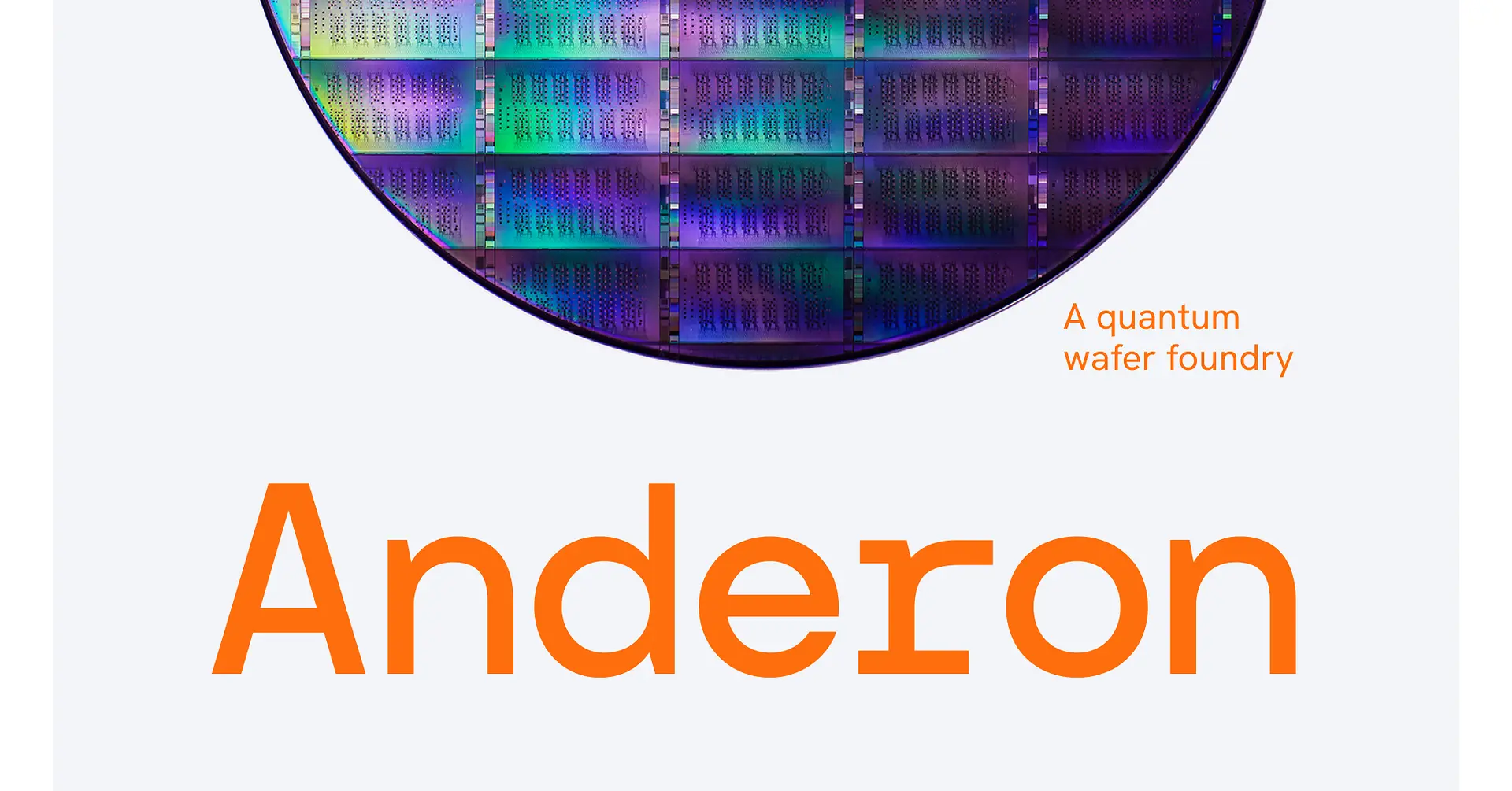
Anderon, a newly established IBM company, will receive $1 billion in funding finalized with the U.S. Department of Commerce to rapidly expand research and development for domestic quantum wafer manufacturing. The investment supports Anderon’s 300-millimeter pure-play foundry, supplemented by an additional $1 billion directly from IBM, signaling a substantial commitment to scaling quantum technology beyond experimental sizes. The company has already begun running quantum wafers through its New York facility, aiming to translate research into commercial technologies.
$1 Billion CHIPS Award Fuels Anderon’s Quantum Wafer R&D
Anderon is already processing quantum wafers at its New York facility, demonstrating a rapid transition from research to initial production following the finalization of $1 billion in funding from the U.S. Department of Commerce. This early activity signals the company’s capacity to swiftly translate pre-production research into commercially viable quantum wafer technologies, a step important for scaling quantum computing beyond experimental stages. The wafers support high-performance superconducting qubit arrays, quantum input/output signaling, and readout signal chain components, foundational elements for diverse quantum architectures, with plans to expand into other modalities in the future.
The $1 billion award, secured through the CHIPS and Science Act, supplements a further $1 billion investment directly from IBM, underscoring a combined commitment to bolstering domestic quantum manufacturing capabilities. Anderon’s operation of a 300-millimeter pure-play foundry distinguishes it from facilities focused on smaller, experimental chip sizes, indicating a clear intent to address the demands of a growing quantum market.
IBM’s internal quantum roadmap necessitates a scalable manufacturing base to maintain its pace of innovation, according to Jay Gambetta, Director of IBM Research & IBM Fellow. “IBM’s quantum roadmap requires a manufacturing foundation that can scale at the pace our work demands,” Gambetta stated. Anderon’s focus on wafer fabrication, rather than complete quantum computer assembly is a deliberate strategy.
“Anderon’s focus on wafer fabrication gives us exactly that and strengthens our ability to execute and accelerate progress toward the next era of quantum computing,” Khare added, explaining the division’s role within the IBM ecosystem. The potential impact of scalable quantum computing extends across multiple sectors, including materials science, chemistry, optimization problems, and cybersecurity, making a reliable domestic wafer supply critical for realizing these advancements.
Anderon intends to provide the advanced manufacturing foundation needed to produce quantum wafers at a production scale, fostering innovation, strengthening supply chains, and supporting the growth of a complete quantum ecosystem. Further details on its capabilities and future plans are available on the company’s website, anderon.com.
IBM’s quantum roadmap requires a manufacturing foundation that can scale at the pace our work demands.
Jay Gambetta, Director, IBM Research & IBM Fellow




See today’s quantum computing news on Quantum Zeitgeist for the latest breakthroughs in qubits, hardware, algorithms, and industry deals.