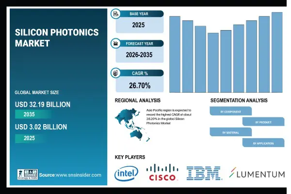
The United States silicon photonics market is poised for rapid expansion, projected to reach approximately $10.76 billion by 2035 from a valuation of roughly $1.00 billion in 2025. This ten-fold increase reflects growing demand for high-speed data transfer driven by artificial intelligence data centers, cloud infrastructure, and 5G networks.
As modern AI training clusters scale, traditional electrical connections are proving insufficient; silicon photonics offers optical interconnects that lower latency and reduce power consumption, enabling efficient data transmission. This growth is fueled by cooperation between chip makers, foundries, and hyperscale data centers seeking alternatives to standard optical modules.
U.S. Silicon Photonics Market Projected to Reach $10.76 Billion by 2035
The U.S. This expansion is particularly evident within the United States, mirroring the overall trend but demonstrating strong domestic investment. Ayar Labs, a San Jose-based company founded in 2015 as a spin-out from MIT, is developing and manufacturing silicon photonics-based chiplets for high-bandwidth, low-latency in-package optical interconnects. The company’s approach integrates optical components directly onto silicon chips, reducing energy consumption and increasing data transfer speeds, and partners with major foundries like GlobalFoundries, TSMC, Intel, and AMD for high-volume manufacturing.
This collaboration enables the scaling of silicon photonics technology beyond the limitations of traditional optical transceiver modules and facilitates co-packaging of optics closer to processors and switching ASICs. The commercial viability of these designs is gaining traction as large-scale data center providers seek alternatives to conventional optical solutions, creating opportunities in areas like advanced packaging, optical engines, and hybrid semiconductor-photonics integration.
Ayar Labs recently secured over $500 million in funding, including a $155 million Series D round led by Intel, AMD, and Nvidia, signaling confidence in the company’s ability to deliver commercial offerings between 2026 and 2028 for AI infrastructure and data center applications. This investment will support the expansion of Ayar Labs’ team and global presence, with new offices in Taiwan and San Jose established to bolster AI infrastructure development.
Beyond hyperscale data centers, applications in high-performance computing, telecommunications, quantum computing, health sensors, automotive industries, and industrial automation are further expanding the market opportunity. The demand for faster and more compact photonic technology is driving growth beyond the traditional optical transceiver market, creating a parallel opportunity for photonics providers.
According to the market report, “Commercialization of such designs is becoming widespread since the providers of large-scale data centers look for substitutes for standard optical transceiver modules.” This shift is not without challenges, however, as component supply remains relatively concentrated, potentially leading to limitations and extended qualification periods. Silicon photonics businesses are therefore competing on production volumes and supply chain resilience, alongside factors like optical integration density, power efficiency, compatibility with semiconductor manufacturing processes, and hybrid material integration. Ayar Labs’ TeraPHY optical I/O chiplet, featuring 70 million transistors and over 10,000 optical devices per chip, exemplifies this push for integration and density.
The company’s partnership with Nvidia, established in 2023, has already seen the integration of Ayar Labs’ optical I/O into Nvidia data center systems for AI and quantum computing acceleration, demonstrating the practical application of this technology. The increasing investment in AI infrastructure and the growing demand for bandwidth are reshaping the silicon photonics landscape, positioning the U.S. market for substantial growth over the next decade.



See today’s quantum computing news on Quantum Zeitgeist for the latest breakthroughs in qubits, hardware, algorithms, and industry deals.