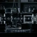


A new integrated photonic architecture for applications including artificial intelligence, sensing and quantum computing is now available, demanding increasingly dense and reprogrammable photonic devices. Matthew Zimmermann at The MITRE Corporation, and colleagues at University of Colorado Boulder, Sandia National Laboratories, Wyant College of Optical Sciences and Research Laboratory of Electronics, have demonstrated a fully monolithic platform integrating piezo-optomechanical photonic integrated circuits with CMOS electronics. This advance enables wafer-scale fabrication of these circuits, utilising over 2 million electrical connections per die, and introduces segmented components functioning as photonic digital-to-analogue converters. By directly constructing photonic wafers on completed CMOS driver wafers, the team achieve dense, scalable electronic control of piezo-optomechanical circuits, representing a key step towards high-density, low-power photonic systems.
High-density piezo-optomechanical photonic integrated circuits via monolithic CMOS fabrication
Over 2 million electrical connections per die were achieved, representing a six-fold increase over previous methods limited by sparse connections and discrete assembly. This significant density, enabled by a 6.4×6.4 micron electrode pitch, had previously been unattainable due to the inherent difficulties of co-integrating electronic drivers with photonic devices in a single, scalable process. Traditional approaches relied on ‘pick-and-place’ techniques for bonding photonic chips to electronic substrates, introducing limitations in bandwidth, power consumption, and overall system size. These discrete assembly methods also suffered from alignment inaccuracies and increased parasitic capacitance, hindering high-speed operation. Directly fabricating photonic wafers onto existing CMOS electronic chips circumvented these limitations in electrical control and interconnection that have long hindered the development of high-density, reprogrammable photonic integrated circuits. The ability to directly address individual photonic elements with many electrical signals is crucial for complex signal processing and advanced optical functionalities.
A monolithic platform now supports wafer-scale integration of piezo-optomechanical photonic integrated circuits, introducing segmented components functioning as photonic digital-to-analogue converters for precise optical control. Each die contains a high-density digital backplane with over 2 million independently-driven electrodes, achieving an electrode pitch of just 6.4 microns. This fine pitch allows for extremely precise control over the optical properties of the integrated photonic circuits. A 200 millimeter photonic wafer is constructed on top of a completed CMOS driver wafer using back-end-of-line processing, establishing electrical connections to integrated piezoelectric actuators beneath silicon nitride waveguides. Silicon nitride was chosen for its high refractive index contrast, low optical loss, and compatibility with CMOS fabrication processes. The piezoelectric actuators, when driven by the CMOS electronics, mechanically deform the waveguides, modulating the optical phase and amplitude of the light propagating through them. This allows for dynamic control of optical signals without requiring external optical components.
Wafer-scale testing verified uniformity and yield across 129 die instances, though the current demonstration focuses on basic device functionality and does not yet address the complexities of integrating these chips into larger, functional systems. Phase shifters, interferometers, and resonators were successfully controlled using a standard HDMI interface. This demonstrates the compatibility of the integrated circuits with existing electronic infrastructure and simplifies the process of prototyping and testing. This achievement unlocks possibilities for complex photonic circuits needed in artificial intelligence and sensing applications, and brings piezo-optomechanical photonic integrated circuits closer to practical use due to their low power consumption and compatibility with very cold temperatures. The low power consumption is particularly important for applications requiring large-scale photonic systems, such as data centres and edge computing devices. Cryogenic compatibility opens up opportunities for quantum computing applications, where maintaining extremely low temperatures is essential for qubit coherence.
Monolithic piezo-optomechanical photonic integrated circuits via back-end-of-line processing
Back-end-of-line processing was central to this advance, enabling the direct construction of photonic wafers onto completed CMOS driver wafers; this is akin to sculpting a complex electronic system from a single block of stone rather than assembling separate pieces. This approach avoids the limitations of front-end-of-line integration, which can expose sensitive CMOS circuitry to harsh fabrication conditions. Creating tiny holes in a passivation layer on the electronic chip allowed access to metal electrodes, which were then filled with material to form vertical interconnects, or vias, between the electronic circuitry and the optical components. These vias provide a low-resistance electrical pathway between the CMOS drivers and the piezoelectric actuators. The fabrication process involved temperatures around 400° C and utilised vertical interconnect access to link the electronic and photonic layers, ensuring the underlying CMOS electronics remained undamaged throughout the process. Maintaining the integrity of the CMOS electronics is critical for ensuring the reliability and performance of the integrated circuits. The resulting chips contain electrodes spaced 6.4 by 6.4 microns apart, demonstrating a strong increase in connection density.
Wafer-scale photonic circuit integration surpasses two million electrical connections per die
Increasingly complex photonic circuits demand tighter electronic control, yet scaling these systems remains a formidable challenge. The demand for greater computational power and bandwidth is driving the need for more sophisticated photonic integrated circuits. While uniformity and yield were established across multiple test structures, quantifying these metrics is vital for assessing the viability of mass production and the potential for cost-effective deployment. Detailed statistical analysis of wafer-scale yield is ongoing to determine the process capability and identify potential areas for improvement. Despite acknowledging that quantifying uniformity and yield across such large wafers presents ongoing challenges, this demonstration of wafer-scale integration represents a major step forward. The team at Massachusetts Institute of Technology, in collaboration with University of Colorado Boulder and Sandia National Laboratories, successfully integrated piezo-optomechanical photonic integrated circuits with conventional CMOS electronics on a single wafer. This monolithic fabrication establishes a platform exceeding two million electrical connections per die, enabling unprecedented control over optical components and translating electronic signals into precise optical modulation. This level of control is essential for implementing complex optical algorithms and achieving high-performance photonic systems. The ability to individually address and modulate millions of optical elements opens up new possibilities for applications in areas such as optical neural networks, high-resolution imaging, and advanced sensing.
The researchers successfully created a monolithic platform integrating photonic and CMOS electronic components on a 200 millimeter wafer, achieving over two million electrical connections per die. This advance matters because it allows for significantly denser and more precise control of optical devices on a single chip. The resulting circuits demonstrate parallel control of optical components using a standard HDMI interface, enabling complex optical signal modulation. Ongoing work focuses on quantifying the uniformity and yield of these large-scale wafers to further refine the fabrication process.
👉 More information
🗞 Monolithic Integration of Piezo-Optomechanical Photonics and CMOS Electronics
✍️ Matthew Zimmermann, Aileen Zhai, Andrew J. Leenheer, Julia Boyle, Mayank Mishra, Daniel Dominguez, Matthew Koppa, Wolf Jehle, Christopher Panuski, Mark Dong, Gerald Gilbert, Dirk Englund and Matt Eichenfield
🧠 ArXiv: https://arxiv.org/abs/2607.01514


See today’s quantum computing news on Quantum Zeitgeist for the latest breakthroughs in qubits, hardware, algorithms, and industry deals.