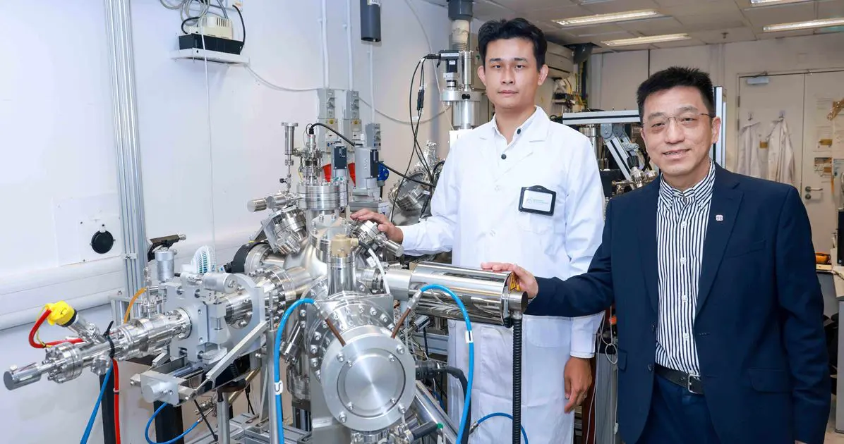
Researchers at The Hong Kong Polytechnic University (PolyU) have engineered a new transistor that operates with a gate-voltage range of only 160 mV, a substantial reduction from the 800 mV traditionally required. The team, led by Jianhua Hao, Head at PolyU, overcame the Boltzmann tyranny, a long-standing physical restriction on transistor energy efficiency, by utilizing quantum tunnelling instead of thermionic emission.
Hao says the transistor is a fundamental building block for future computing and enables ultra-low-power, high-performance integrated circuits essential for emerging AI chips and advanced semiconductor applications. The device, fabricated from 2D bismuth and indium selenide layers, is detailed in a recent publication in Science.
This breakthrough addresses a critical limitation in conventional transistors known as the Boltzmann tyranny, a long-standing physical restriction on energy efficiency. The device relies on an ultra-thin heterostructure fabricated from alternating layers of 2D bismuth (Bi) and indium selenide (InSe) created using a technique called pulsed laser deposition (PLD).
This precise layering transforms semi-metallic bismuth into a semiconductor in its 2D form, establishing ideal energy band alignment for efficient charge carrier tunnelling into the indium selenide. Conventional complementary metal-oxide-semiconductor field-effect transistors (MOSFETs) depend on thermionic emission, which has a minimum gating voltage of 60 millivolts (mV); however, the Boltzmann tyranny prevents subthreshold swing (SS) values below 60 mV decade⁻¹ at room temperature, hindering further advancements in high-performance electronics.
Jianhua Hao said the International Roadmap for Devices and Systems (IRDS) has identified TFETs as the most promising alternative to MOSFETs. By utilizing quantum tunnelling, the new 2D heterostructure transistor circumvents this 60 mV decade⁻¹ boundary, exceeding the standard MOSFET limit.
The resulting Bi/InSe TFET achieved SS values well below the thermionic limit across six orders of magnitude of current switching, and crucially, delivered a high output current of up to several microamps per micrometre (μA μm⁻¹). This high output current is essential for driving multiple downstream logic gates, reducing circuit delay and ensuring compatibility with existing integrated circuit (IC) chips, a challenge that previous experimental TFET designs often failed to meet.
This is particularly significant because PLD offers seamless integration with traditional silicon-based manufacturing processes, providing a scalable roadmap for energy-efficient microchips and specialized hardware for artificial intelligence (AI) applications. The device operates at room temperature on standard centimetre-scale silicon substrates, further enhancing its potential for widespread adoption. The team’s work suggests a path toward overcoming fundamental physical limitations in transistor design, potentially unlocking new levels of performance and efficiency in the next generation of microelectronics.



See today’s quantum computing news on Quantum Zeitgeist for the latest breakthroughs in qubits, hardware, algorithms, and industry deals.