

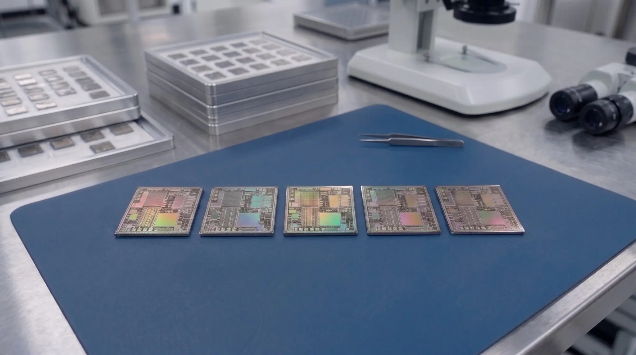
A four-inch wafer will soon be central to metalens prototyping efforts at the University of Arizona, as MetaOptics prepares to deploy its Direct Laser Writer (“DLW”) at the Center of Semiconductor Manufacturing. This installation, expected to begin in 2027, marks a key step in MetaOptics’ U.S. expansion and will allow prospective customers to observe the system firsthand. Dr. Krishna Muralidharan of the University of Arizona’s Department of Materials Science and Engineering will guide collaborative research and evaluation using the deployed DLW, supporting small-volume production and faster iteration cycles. MetaOptics expects the deployment to generate user feedback and the company stated that the deployment of its DLW is a key milestone for MetaOptics’ U.S. expansion strategy, prospective U.S. customer engagement, and commercialization roadmap.
Direct Laser Writer Deployment at University of Arizona’s Center
This installation represents a significant expansion of MetaOptics’ presence in the United States and a commitment to collaborative research with leading semiconductor experts. The agreement, finalized on July 21, 2026, establishes a pathway for faster iteration cycles and streamlined development of metalens technology for both academic and commercial applications. Installation of the DLW is anticipated to begin in 2027, defining a timeline for this strategic U.S. initiative. The system’s ability to handle a four-inch wafer is central to its capabilities, a size chosen to facilitate rapid prototyping and small-volume production. This scale allows partners to move efficiently from initial concept to tangible product, addressing a critical bottleneck in the development of advanced optical components.
The deployment will offer prospective customers a firsthand view of the technology, allowing them to assess its potential for their specific metalens prototyping needs. Dr. Krishna Muralidharan’s guidance will be crucial in harnessing the system’s capabilities and generating valuable insights into metalens fabrication and performance. MetaOptics anticipates that this collaboration will yield critical user feedback and technical validation of its equipment and products, directly supporting emerging U.S. efforts in silicon photonics, co-packaged optics, and integrated photonics, areas where metalens technology offers a compelling advantage in the market.



See today’s quantum computing news on Quantum Zeitgeist for the latest breakthroughs in qubits, hardware, algorithms, and industry deals.