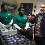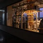

Adam Wei Tsen has been appointed an Endowed Chair in Nanotechnology at Waterloo, a position he will hold for five years with potential for renewal, recognizing his research bridging materials science and device engineering. Tsen’s team engineers heterostructures by stacking two-dimensional quantum materials, creating devices intended to outperform traditional systems in electronic, magnetic, or optical functions. Tsen states that the university’s unique nanotechnology infrastructure and collaborative strengths are essential to fabricating devices on an extremely small scale. This appointment signals continued institutional investment in nanoscale device building and interdisciplinary research.
Two-Dimensional Quantum Materials Enable Heterostructure Engineering
Tsen’s team constructs these layered materials by stacking atomically thin materials, tailoring their properties to create devices demonstrating novel electronic, magnetic, and optical functionalities that, in some cases, exceed the performance of conventional systems. This precise construction demands capabilities beyond standard materials research, requiring electrical contacts to be formed on materials measured in microns.
The success of this interdisciplinary work relies heavily on collaborative expertise; Tsen explains, “Someone from a purely chemistry or physics background might not have a lot of exposure to devices and circuits. Someone from an engineering background might not know much about solid-state materials.” His team integrates researchers from chemistry, physics, and engineering, and their combined skills are crucial for navigating the complexities of both fundamental materials science and practical device engineering.
This approach allows for adaptation of techniques developed for two-dimensional systems to other materials, including bulk crystals and thin films, broadening the scope of potential applications. “We need to use the nanofabrication facilities to make electrical contacts and build complex heterostructures.
Without that infrastructure, we wouldn’t be able to do the things that we do at all.” He further emphasizes the importance of bridging traditionally separate research communities, asserting, “I think our work can connect the materials, nanotechnology, quantum, and device communities more broadly.” The combination of specialized facilities and a diverse research team positions Waterloo as a key hub for nanoscale device development and quantum materials research.
The nanotechnology infrastructure here is quite unique in Canada.
Adam Wei Tsen, Associate Professor in Chemistry and faculty at the Institute for Quantum Computing


See today’s quantum computing news on Quantum Zeitgeist for the latest breakthroughs in qubits, hardware, algorithms, and industry deals.