
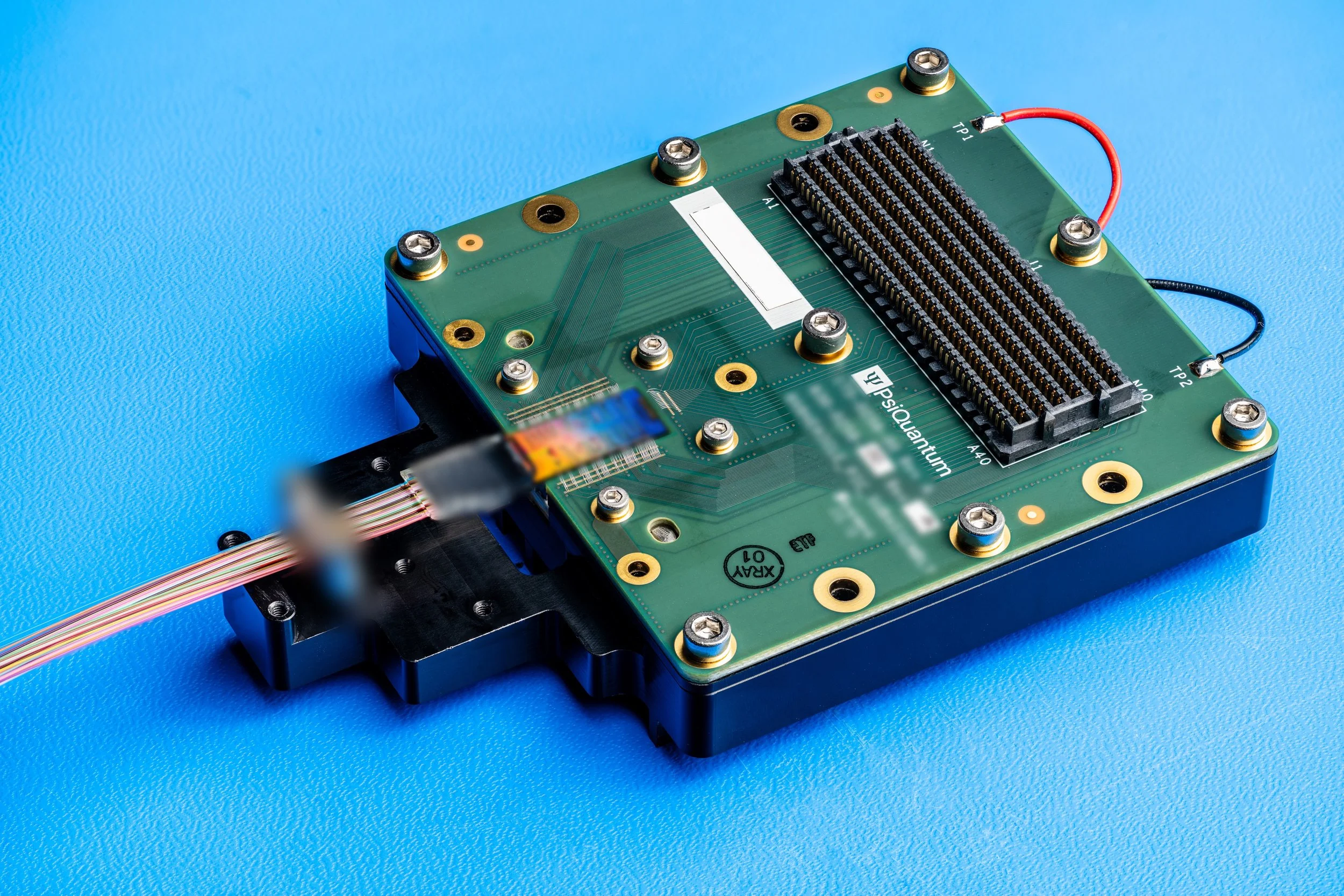
Has demonstrated an 8×8 radix Optical Circuit Switch, achieving 1.2 dB of insertion loss in testing, a performance level the company reports is typical. This low-loss silicon photonics platform, initially developed for quantum computing, now addresses escalating demands for faster data transfer in artificial intelligence infrastructure. Testing showed reconfiguration times of less than 3 ms without amplification, exceeding initial targets. “As AI computing pushes infrastructure to its limits, we now have an opportunity to put our technology to work today,” said Victor Peng, Chief Executive Officer of PsiQuantum.
Low-Loss Silicon Photonics Validates AI Infrastructure Scaling
The 8×8 radix Optical Circuit Switch demonstrated by PsiQuantum achieves an insertion loss of 1.2 dB during testing, a figure the company reports is typical and positions the technology as a leading solution for scaling AI infrastructure. This low loss is critical because it minimizes signal degradation as data travels through the switch, enabling faster and more reliable communication between the increasingly large compute pools driving modern AI applications.
The company’s approach focuses on maintaining signal integrity even as data demands escalate, a challenge that has prompted the computing industry to explore optical solutions for improved connectivity, PsiQuantum says. The demonstrated switch builds on a silicon photonics platform developed over nearly a decade for utility-scale quantum computing, reflecting the convergence of these two demanding fields. PsiQuantum is now sharing samples of this demonstration vehicle with prospective customers, signaling an advancement toward commercial products planned for announcement in the coming months.
This move reflects a strategy of addressing fundamental scaling problems early in the development process, allowing the technology to be adapted for immediate use in AI infrastructure while still supporting the long-term goal of building fault-tolerant quantum computers. This speed is particularly noteworthy, as it allows for rapid switching between different data paths, minimizing latency and maximizing throughput in demanding AI systems.
“AI is driving extraordinary growth in the scale and complexity of computing infrastructure, and optics will play an increasingly important role in enabling that growth,” said Rob Soderbery, Executive Vice President. The development of barium titanate (BTO) integration at the 300mm wafer scale demonstrates a commitment to advanced materials science, though BTO was not used in the current demonstration vehicle.
The company’s use of BTO in its quantum systems highlights a future path toward even faster and more advanced products, providing an additional layer of scalability and performance, according to PsiQuantum. The company’s work aligns with a broader trend of government investment in domestic quantum computing capabilities; in September 2026, PsiQuantum signed documentation with the U.S. Department of Commerce to accelerate research and development, domestic manufacturability and performance of its critical components.
“PsiQuantum has spent nearly a decade developing silicon photonics against some of the most demanding requirements imaginable. What we are demonstrating today is that this platform can deliver exceptional performance for optical circuit switching for AI computing,” said a company spokesperson. The platform is designed to use high-volume semiconductor manufacturing, existing cryogenic infrastructure and architectural flexibility to rapidly scale its systems, offering a viable path toward building and deploying useful quantum computers.
This opportunity exists because we chose to solve the hardest scaling problems at the beginning of our roadmap to utility-scale quantum computing.
Victor Peng, Chief Executive Officer of PsiQuantum



See today’s quantum computing news on Quantum Zeitgeist for the latest breakthroughs in qubits, hardware, algorithms, and industry deals.