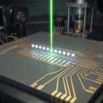


King Abdullah University of Science and Technology (KAUST), located in Thuwal, Saudi Arabia, is collaborating with the Massachusetts Institute of Technology to fabricate a CMOS platform for analyzing quantum materials. Researchers, including Sharad Kumar Yadav of KAUST and Luca Nessi of MIT, who contributed equally to this work, have demonstrated that a standard 65-nanometer CMOS process, typically used for microchip fabrication, can be repurposed as a scalable platform for multimodal quantum materials characterization. The integrated system, occupying a mere one square millimeter, enables microwave, electrical, thermal, optical, and structural analysis without requiring sample-specific fabrication. This work establishes a foundry-manufacturable platform for quantum sensing and materials characterization, offering a path toward increased reproducibility and scalability in the field.
Foundry CMOS Platform for Multimodal Characterization
A standard semiconductor manufacturing process is now enabling new advances in quantum materials analysis, as researchers demonstrate a foundry-compatible CMOS platform for multimodal characterization. This is a significant departure from traditional methods, which rely on assembling discrete hardware components, a process that limits reproducibility and complicates measurements, particularly for air-sensitive materials at cryogenic temperatures. As the paper notes, modern quantum materials experiments increasingly rely on microwave, electrical, thermal, optical, and structural probes, but these capabilities are often hampered by custom hardware limitations. The platform’s design addresses five key requirements: efficient field generation, electrical and thermal interfacing, optical accessibility, compatibility with structural imaging, and reproducible fabrication through commercial semiconductor manufacturing. Validation of the platform involved three representative applications.
Researchers achieved over 20% contrast in NV-center optically detected magnetic resonance (ODMR) at microwave powers of 4, 9 dBm, a reduction of 20, 25 dB compared to conventional antenna-based approaches while maintaining sensitivities of 2-3 Tesla per root Hertz. The integrated RF architecture enabled cryogenic magnetic susceptibility measurements of Fe3GeTe2 heterostructures at 1.75 Kelvin without requiring sample-specific fabrication. Importantly, the platform also demonstrated compatibility with in-situ electron-beam imaging, showing no measurable degradation in image quality upon device operation. These results establish a scalable, foundry-manufacturable platform for multimodal quantum sensing and materials characterization. The use of a commercial TSMC 65-nm RF CMOS process, with its heterogeneous back-end-of-line stack, proved crucial, allowing for the functional partitioning of the metal layers to create the necessary subsystems.
Traditionally, these capabilities have been built from custom hardware, hindering reproducibility and scalability. This partnership highlights an increasingly international distribution of advanced materials research, extending beyond established US and European centers. The team’s innovation centers on a 65-nanometer CMOS platform, typically used for standard microchip production, now adapted to serve as a versatile characterization tool. The resulting architecture, detailed in recent work, functionally partitions the metal stack within a 1 mm² footprint into microwave, thermal, and electrical subsystems; this compact design is crucial for cryogenic measurements and compatibility with sensitive materials, and 1.75 K represents a significant simplification of experimental setup.
While many quantum sensing techniques demand isolation from external interference, this platform demonstrates compatibility with direct observation via in-situ electron-beam imaging, a technique typically considered disruptive to sensitive measurements. Researchers successfully operated the CMOS platform within the electron microscope, a feat previously requiring significant engineering workarounds. This approach allows for simultaneous materials analysis without sample-specific fabrication, and the ability to perform in-situ electron-beam imaging alongside quantum sensing opens new avenues for materials discovery and analysis; researchers can now directly observe changes in a material’s structure as it responds to external stimuli, such as microwave fields or temperature variations, providing a more complete understanding of its properties.
This partnership isn’t simply about pooling expertise. The core of this innovation lies in repurposing a 65-nanometer CMOS platform, the same technology used to manufacture standard microchips, for the far more demanding task of multimodal quantum materials characterization. This platform integrates microwave delivery, electrical interfacing, and thermal control, all while maintaining compatibility with cryogenic temperatures down to 1.75 Kelvin, optical spectroscopy, and electron microscopy.
👉 More information
🗞 Foundry CMOS platform for multimodal quantum materials characterization
✍️ Sharad Kumar Yadav et al.
🧠 ArXiv: https://arxiv.org/abs/2607.18059



See today’s quantum computing news on Quantum Zeitgeist for the latest breakthroughs in qubits, hardware, algorithms, and industry deals.