

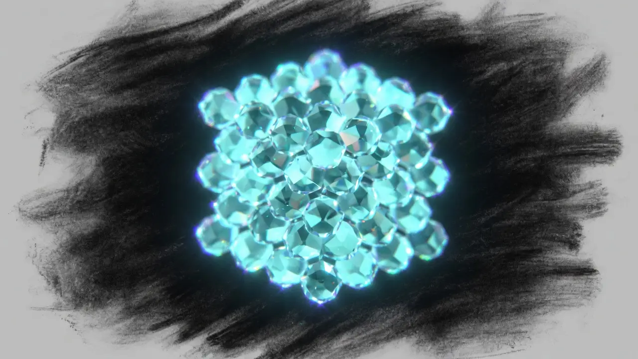
Researchers have achieved up to a 45-fold increase in the photoluminescence of boron vacancies in hexagonal boron nitride at 4 Kelvin using a novel van der Waals heterostructure. The work demonstrates a mechanism where light absorbed by lead iodide drives excitation of the boron vacancy defect, boosting signal strength without compromising its spin properties. This coupling, enabled by a type-I band alignment at the lead iodide-hBN interface, facilitates efficient energy transfer and improved sensitivity to external magnetic fields, establishing a route for amplifying weak quantum defect signals in nanomaterials.
Van der Waals Heterostructure Enhances Boron Vacancy Emission
This stacked structure, comprised of hexagonal boron nitride, a boron vacancy layer, and lead(II) iodide, uses a mechanism to amplify the typically weak signal emitted by the boron vacancies without compromising their spin properties. The design relies on the efficient transfer of energy from the lead iodide to the boron vacancy, effectively increasing the number of emitted photons. The heterostructure’s performance stems from a specific energetic alignment and spectral overlap between the materials, enabling interlayer coupling that facilitates this energy transfer.
This process circumvents the usual limitations imposed by the dipole-forbidden transition between the ground and excited states of the boron vacancy, which typically results in low quantum efficiency. Photoluminescent excitation data confirm this increased defect emission when excited with energies lower than the lead iodide bandgap. Further analysis revealed that the coupling between the layers also impacts the defect lifetime, a critical parameter for sensing applications.
Conversely, at room temperature, the coupled region displayed a shorter lifetime under 555 nanometer excitation, potentially due to increased contributions from broadband emission associated with the lead iodide. These measurements were performed using an intensity-weighted average lifetime, fitted with IRF-deconvoluted biexponential functions. The team assessed the heterostructure’s performance at room temperature to evaluate its suitability for practical sensing under ambient conditions, finding the same characteristic donor quenching and acceptor enhancement observed at 4 Kelvin.
Fluorescence resonance energy transfer is favorable in the coupled structure, supported by experimental emission and absorption spectra. The atomically thin and chemically accessible surface of hBN offers advantages for close sensor-sample contact, as demonstrated by optical monitoring of interfacial reactions and quantum detection of paramagnetic species in liquids. The work does not seek to modify the intrinsic emission process of the defect, but rather to introduce alternative pathways for optical absorption.
Type-I Band Alignment Facilitates Photon-Ratchet Mechanism
A type-I band alignment between lead iodide (PbI2) and hexagonal boron nitride (hBN) creates conditions for a photon-ratcheting mechanism, enabling excitation of boron vacancies (VB⁻) within the hBN layer. This coupling, achieved through van der Waals heterostructure fabrication, facilitates a nonlinear polarization generated by optical absorption in the PbI2, effectively driving the excitation of the defect. Calculations reveal minimal disruption to the electronic and spin structure of the VB⁻ defect during this process, preserving the integrity of optically detected magnetic resonance (ODMR) contrast, a key factor for sensitive magnetic field detection.
The four-layer heterostructure, comprising hBN capping layers, a VB⁻ layer, and a PbI2 layer, uses both energetic alignment and spectral overlap to promote interlayer coupling. This arrangement allows for efficient energy transfer from the PbI2 to the VB⁻ defect, a process confirmed by theoretical modeling and supported by experimental observations.
The observed increase in absorption by the heterostructure at energies below the PbI2 band gap, as demonstrated in differential reflectance scans performed at 4 Kelvin, further validates the energy transfer pathway. Theoretical calculations of the spin density distribution at the defect confirm that the coupling to PbI2 largely preserves the VB⁻ defect’s spin characteristics. The calculated spin-resolved band structures, detailed in the Supplementary Information, demonstrate minimal alteration to the defect’s electronic and spin structure, consistent with the retention of ODMR resonance positions and the preservation of spin-dependent optical readout.
Simplified modeling using a seven-by-seven spin Hamiltonian further supports these findings, showing minimal changes in eigenstate composition and basis-state mixing before and after PbI2 coupling. The band alignment, determined by Kelvin Probe Force Microscopy (KPFM) performed in vacuum, places the band gaps around the Fermi levels, promoting energetically favorable excitation transfer from PbI2 to VB⁻.
The KPFM measurements, overlaid on scanning electron microscopy (SEM) images, provide a detailed map of the Fermi level across the heterostructure. While reverse transfer of energy into PbI2 free-exciton or band-edge states is energetically unfavorable, the possibility of red-shifted localized PbI2 states acting as acceptor states remains a consideration. However, the observed VB⁻ enhancement strongly suggests that such reverse transfer does not significantly contribute to the overall process.
The fabrication process involved referencing each frame independently to account for Au contamination before stitching them together to create a complete mosaic. Translational alignment of common features within overlapping regions ensured accurate registration, and a line-dependent Au correction, applied separately to all nine complete frames, resulted in a minimal change of only 4-15 meV in the reported region-averaged values. This meticulous approach ensured the precision of the KPFM measurements, with a stated precision of 0.1 electron volts.
The observed effects demonstrate a pathway to amplify the signal from boron vacancies, potentially unlocking new capabilities in quantum sensing and nanoscale magnetometry. The team’s work highlights the potential of carefully engineered van der Waals heterostructures to manipulate light-matter interactions at the nanoscale.
Boron Vacancy (VB⁻) as a Quantum Sensing Platform
The observed enhancement is not merely an increase in brightness; it translates to a demonstrable improvement in the sensitivity of the VB⁻ defect to external magnetic fields, a critical parameter for nanoscale sensing precision. Researchers confirmed that the observed increase in photoluminescence is concurrent with a suppression of free-exciton emission within the lead iodide itself, providing direct evidence for this energy transfer process.
Excitation-dependent photoluminescence and absorption measurements further support a contribution from nonlinear optical coupling, aligning with theoretical calculations based on density functional theory. Beyond the low-temperature performance, the heterostructure maintains a significant advantage even at room temperature, exhibiting a 4 to 15-fold increase in emission intensity.
This persistence of enhancement under ambient conditions is important for practical sensing applications, as many real-world scenarios require operation outside of cryogenic environments. Continuous-wave optically detected magnetic resonance measurements demonstrate that this improved emission translates to a tangible gain in magnetic sensitivity, observed across multiple excitation wavelengths at room temperature.
The system was excited off-resonantly by either a 488 nm or 555 nm laser, and in both cases, a strong improvement of the photoluminescence signal was observed in the heterostructure region while retaining the same resonant features as in the VB⁻ region. The ability to systematically engineer these heterostructures opens avenues for amplifying weak signals from ultrathin or low-defect-density sensing layers, potentially leading to new possibilities for quantum sensing in diverse materials.
The researchers note that the approach yields substantial enhancement of both photoluminescence and sensing performance of the VB⁻ defect, establishing a generalizable materials strategy for optical enhancement of quantum defects and engineering spin-photon interfaces in ultrathin quantum sensing platforms. “Overall, these measurements and calculations demonstrate that directed vdW heterostructure engineering can provide a materials platform that enables optically mediated excitation of spin defects through nonlinear photon-mediated excitation and interlayer energy transfer from PbI2 to VB⁻ defects in hBN, with possible contributions from other short-range coupling channels,” the paper states.
Reciprocal photoluminescence mapping further validated the energy transfer mechanism, revealing a clear correlation between the suppression of lead iodide emission and the amplification of boron vacancy luminescence. This observation supports the hypothesis that the lead iodide layer is not simply acting as a light concentrator, but rather actively participating in the excitation process.
The enhancement persists even in regions with relatively low defect density, suggesting that the photon-ratcheting mechanism is robust and scalable. This is an important distinction, as altering the defect’s inherent properties could potentially compromise its quantum coherence and sensing capabilities.
Challenges with Integrating 2D Spin Defects into Devices
The team’s work demonstrates that the engineered van der Waals heterostructure not only amplifies the signal from boron vacancies but also improves the performance of the resulting quantum sensor, a key step toward practical devices. The heterostructure’s design uses interlayer optical coupling to achieve this enhancement, a mechanism supported by both experimental data and density functional theory calculations. This energy transfer process effectively channels light absorbed by the PbI₂ layer to excite the VB⁻ defect, increasing its emission intensity without altering the defect’s intrinsic quantum properties.
Devices tested exhibited a 45-fold increase in photoluminescence intensity at 4 Kelvin, with enhancements ranging from 4 to 15-fold persisting even at room temperature. The team notes that the largest room-temperature differential enhancement measured across devices was 15-fold, demonstrating the robustness of the effect. The combination of neutron irradiation and careful heterostructure assembly allows for the creation of highly sensitive quantum sensors with enhanced performance characteristics.

See today’s quantum computing news on Quantum Zeitgeist for the latest breakthroughs in qubits, hardware, algorithms, and industry deals.