
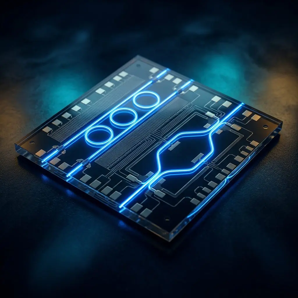
Harvard University researchers are building a new type of optical device using engineered semiconductors and metasurfaces to efficiently mix and transform near-infrared light, an important advancement for fiber-optic networks and potentially smaller quantum technologies. The collaboration between Harvard SEAS, University of Texas Austin, and University of California, Irvine, detailed in Nature Nanotechnology, moves beyond traditional materials like lithium niobate and gallium arsenide by co-designing layered semiconductors with nanostructured metasurfaces.
“This work combines, in a creative way, quantum engineering of an underlying material and enhancing its nonlinearity, together with optimized metasurface design,” said Professor Federico Capasso. The resulting device concentrates light within its structure, promising more compact and scalable photonic components.
Engineered Multi-Quantum Wells Enhance Nonlinear Light Interaction
Engineered multi-quantum wells amplify nonlinear light interaction to three orders of magnitude higher than unpatterned wafers, potentially revolutionizing photonic circuits. The Harvard SEAS team achieved this enhancement by meticulously layering gallium arsenide and aluminum gallium arsenide into ultra-thin semiconductor stacks, carefully tailoring the electronic energy levels for maximized light-matter interaction. This design utilizes a different electronic transition than traditional methods, enabling strong nonlinear effects at near-infrared wavelengths important for fiber-optic communications.
Researchers also manipulated field symmetry to prevent canceling interactions, further boosting conversion efficiency. Collaborators at the University of Texas at Austin, led by Professor Seth Bank, designed the multi-quantum well material itself, while the Harvard Capasso group focused on electromagnetic field behavior within the structure. “So that it can make the most of the material property,” explained Pernille Undrum Fathi, a Ph. D. student in Capasso’s lab and first author of the published research in Nature Nanotechnology.
This coordinated effort demonstrates a synergistic approach to materials science and nanophotonics. The resulting device’s ability to operate effectively in free-space optics, as noted by the team, “The overall nonlinear response is greatly enhanced and made usable for free-space optics,” suggests a path toward more compact and scalable photonic components for diverse applications, extending beyond the limitations of lithium niobate and gallium arsenide.
so that it can make the most of the material property.
Pernille Undrum Fathi, a Ph
Metasurface Design Optimizes Frequency Conversion in Semiconductors
Precisely tailoring nanopillars on a metasurface to concentrate light within an engineered semiconductor structure is the core of the team’s design, orienting electromagnetic fields and amplifying light intensity as a departure from conventional frequency conversion methods. This coordinated manipulation of light fields enhances nonlinear interactions, enabling more efficient generation of new light frequencies at specific wavelengths, particularly those used in fiber-optic networks. Beyond simply layering materials, the Harvard SEAS group co-designed the semiconductor layers and the metasurface, ensuring electronic states, optical fields, and geometry all contribute to efficient frequency conversion.
This synergistic approach allows for optimization at a given wavelength, moving beyond the limitations of naturally occurring nonlinear crystals. The precisely patterned nanopillars, a hallmark of the Capasso group’s expertise, function at subwavelength scales to trap and shape light, maximizing its interaction with the semiconductor material.
This integrated design represents a shift in how optical devices are constructed, potentially leading to miniaturized components for diverse applications including telecommunications and quantum communication systems. The researchers report that this method enhances nonlinear frequency conversion by carefully controlling the symmetry of the electromagnetic field, preventing destructive interference and boosting the overall efficiency of the process.
This work combines, in a creative way, quantum engineering of an underlying material and enhancing its nonlinearity, together with optimized metasurface design.
Federico Capasso, the Robert L. Wallace Professor of Applied Physics and Vinton Hayes Senior Research Fellow in Electrical Engineering
Source: https://seas.harvard.edu/news/new-device-design-could-miniaturize-photonics-quantum-technologies



See today’s quantum computing news on Quantum Zeitgeist for the latest breakthroughs in qubits, hardware, algorithms, and industry deals.