

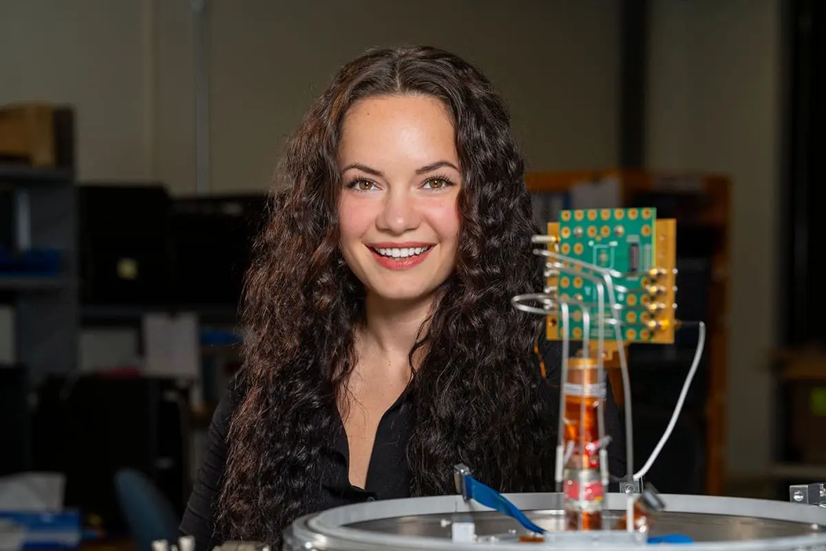
Olivia Seidel, a student within Fermi National Acceleratory Laboratory’s Microelectronics group, is using artificial intelligence to model transistor behavior in extreme cold, directly supporting the U.S. Department of Energy’s Genesis Mission. Transistors, the fundamental building blocks of all electronics, are now so small, just a few nanometers across, that a single wavelength of visible light is hundreds of times wider than the transistors, presenting significant challenges for continued miniaturization. For decades, research focused on room temperature performance, but emerging technologies like quantum computing demand electronics functioning at cryogenic temperatures, just a few degrees above absolute zero. Seidel explains that even a seemingly minor shift in transistor behavior can lead to circuit failure or excessive power consumption in these extreme environments, with implications for both quantum systems and space-based electronics.
AI Accelerates Cryogenic Transistor Modeling for Physics Models
Her work directly supports the U.S. Department of Energy’s Genesis Mission, a national AI initiative combining the resources of national laboratories, research universities, and industry to supercharge American innovation. This shift is driven by the demands of quantum computing, particle physics experiments like those conducted at Fermilab’s DUNE facility, and the unique thermal conditions encountered by satellites in deep space. “For most of that history, room temperature was the only environment that mattered,” Seidel explains, highlighting the novelty of this research direction. The behavior of transistors changes dramatically when cooled to these extremes; specifically, the voltage required to switch a transistor on increases significantly below 4 kelvin [about minus 452 degrees Fahrenheit]. This shift, if unaccounted for, can lead to circuit failure or drastically increased power consumption, a critical concern in cryogenic systems where excess heat can disrupt sensitive quantum states or particle detection.
Seidel isn’t simply measuring this altered behavior; she’s building physics models to predict it. Traditionally, creating a robust cryogenic model for a single transistor type could take around two years. Recognizing this bottleneck, Seidel integrated machine learning into the modeling process. “The idea is to use machine learning to speed up the modeling process enormously,” she states. Her prototype replaces a time-consuming step in conventional modeling with an AI-driven approach, achieving comparable, and sometimes better, results. The machine learning model can predict optimal physics parameters from measurement data in approximately 120 milliseconds, improving upon the weeks or months required by traditional methods. “We’re laying the groundwork so that future researchers don’t have to spend years on something a well-trained model can do in a fraction of the time,” Seidel asserts. This work, part of the Accelerating eXtreme Environment Specs-to-Silicon project, aims to create a complete, AI-built model for transistors used in quantum information science and high-energy physics applications, moving beyond simply adapting room-temperature models.
Transistor Behavior Shifts at Cryogenic Temperatures Below 4 Kelvin
This scaling presents unique challenges, particularly as research expands beyond conventional operating temperatures. Seidel’s work isn’t simply about observing altered behavior; it’s about creating predictive models that circuit designers can rely on. “The goal is that when a circuit designer sits down to build something that needs to operate at 4 kelvin, they can trust the model, rather than building the whole thing, putting it in a cryogenic system and finding out it doesn’t work,” she explains. “Technology advances faster than the models do, and that’s an industry-wide challenge,” she notes. Her prototype leverages machine learning to accelerate this process, replacing a time-consuming step with an AI-driven prediction based on lab measurement data. Seidel envisions a future where models are built inferring underlying physics directly from measurements, a fundamentally more powerful approach to cryogenic transistor modeling.
We’re laying the groundwork so that future researchers don’t have to spend years on something a well-trained model can do in a fraction of the time.
Applications Benefit from Cryogenic Transistor Performance
U.S. Department of Energy’s Genesis Mission combines the expertise of the Department of Energy’s national laboratories, U.S. research universities and industry to supercharge American innovation, and Seidel’s work represents a focused effort to overcome longstanding challenges in cryogenic electronics design. Several applications stand to benefit from more accurate and efficient cryogenic transistor modeling. Trapped ion quantum computers, which utilize charged atoms as qubits, rely on high-voltage transistors operating in extremely cold conditions to precisely manipulate these quantum bits, suppressing thermal noise and preserving qubit stability. Similarly, superconducting nanowire single-photon detectors, used for particle detection and precision measurements, also require cryogenic electronics. Seidel’s prototype, which integrates machine learning into the modeling process, has demonstrated a speedup.
The demand for increasingly sophisticated electronics extends beyond conventional operating temperatures, driving a need for accurate modeling of transistor behavior in extreme cold, and the U.S. Department of Energy’s Genesis Mission is now employing artificial intelligence to dramatically accelerate this process. Historically, modeling these transistors primarily focused on room-temperature performance, but this is changing as new technologies demand more.



See today’s quantum computing news on Quantum Zeitgeist for the latest breakthroughs in qubits, hardware, algorithms, and industry deals.