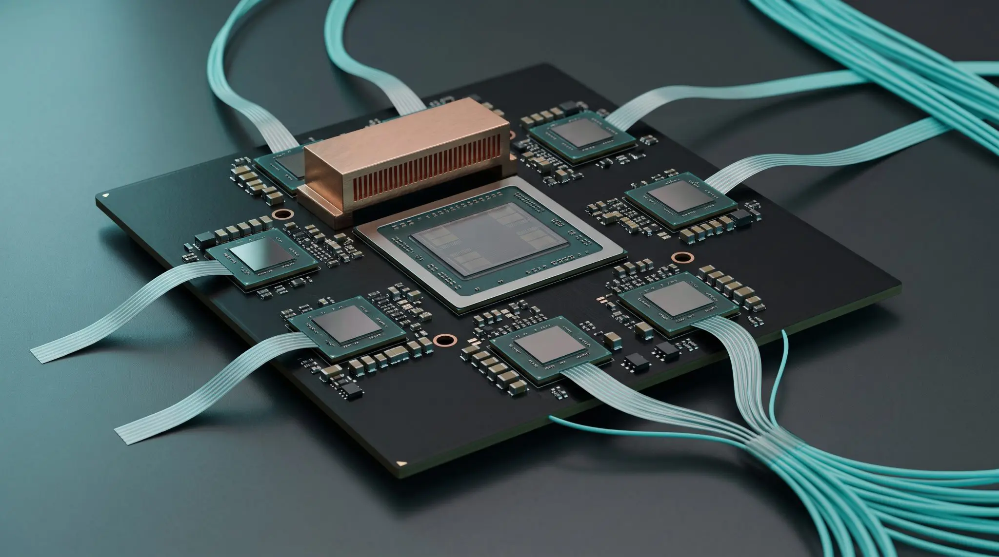
A new quantum magnetometer chip using 4H-silicon carbide achieves a sensitivity of, representing an improvement of two to three orders of magnitude over sensors built with more complex confocal techniques. The device uses industrially scalable wafer-scale fabrication, a departure from the manufacturing challenges of diamond-based quantum sensors. Integrating color center ensembles into a planar silicon carbide waveguide simplifies fluorescence extraction and streamlines optical excitation. The researchers report that this development “paves the way for the development of SiC-quantum sensing technologies.”
4H-SiC Waveguide Design Enables Efficient Fluorescence Extraction
Efficiently channeling the faint glow emitted by quantum sensors has long been a challenge, but a new design using a silicon carbide waveguide significantly simplifies fluorescence extraction. The planar structure, formed as a layered “sandwich” of doped silicon carbide, guides both excitation and fluorescence light from embedded V2 color centers with minimal loss across a broad spectrum from 780 to 1200 nanometers. This contrasts sharply with the complexities of standard confocal methods, which require precise alignment and collection optics.
Fabrication of the chip relies on industrially scalable wafer-scale techniques, culminating in diced chips engineered for low optical surface roughness to minimize coupling losses, as detailed in a related publication. The waveguide’s core layer thickness dictates the number of modes it supports, while a strong refractive index jump between the core and an upper layer confines light, preventing unwanted coupling to structures on the chip’s surface.
This careful control of light propagation is critical for maximizing the signal received from the quantum sensors. Measurements using a custom-built transmission fluorescence setup demonstrate the coherent capabilities of a large ensemble of V2 centers integrated within the waveguide. Researchers observed clear Rabi oscillations, indicating coherent control over an estimated number of V2 centers embedded in the planar structure. These oscillations were achieved using different radio-frequency field amplitudes, confirming the ability to drive the ensemble coherently.
“We observe clear coherent oscillations in fluorescence and thus population in the respective spin states,” the study reports, demonstrating the potential for manipulating the quantum state of a substantial number of color centers simultaneously. This heightened sensitivity is achieved through the efficient extraction of fluorescence, allowing for a stronger signal and more precise measurements of magnetic fields.
Proton implantation techniques were used to generate V2 silicon vacancies, with the method chosen for its ability to precisely control the depth of the implanted ions within the silicon carbide bulk. While the current coil geometry used for radio-frequency excitation lacks optimized homogeneity, it successfully demonstrated the feasibility of the design.
The researchers note that future iterations will benefit from rigorous electromagnetic design to further refine the coil and enhance the sensor’s performance. The team’s work highlights the potential of silicon carbide waveguides to streamline the development and deployment of high-sensitivity quantum sensors for a range of applications.
V2 Color Centers Created via Proton and Electron Implantation
Proton implantation, using an energy of 600 keV, offers precise depth control when generating V2 silicon vacancies within the 4H-silicon carbide, as the particles are fully contained within the material’s bulk and their penetration depth is dictated by the applied energy. This contrasts with electron implantation, where the significantly lower mass of electrons results in a much longer mean free path, allowing them to traverse the entire wafer and create a homogeneous distribution of defects.
Researchers conducted a comparative study of both methods to determine the most effective approach for V2 vacancy creation, an important step in building the quantum magnetometer chip. The team employed a proton implantation dose between and an energy of 400 keV, carefully selected to optimize V2 ensemble generation, while electron irradiation used a dose of to achieve a dense concentration of vacancies.
Following both implantation techniques, all samples underwent high-temperature annealing at for 30 minutes, a process designed to activate the vacancies and minimize residual lattice damage. Depth-resolved mapping of the resulting V2 profiles was then performed using confocal microscopy, reconstructing emitter distributions along the implantation axis to assess the effectiveness of each method. Confocal measurements at the centers of the implanted regions revealed a distinct zero-phonon line at 917 nm, alongside a visible phononic sideband even at 8 Kelvin, confirming the successful creation of V2 color centers.
The comparatively long mean free path of electrons, however, meant no distinct implantation peak was present, resulting in the uniform depth distribution previously predicted. “Based on proton and electron implantation techniques, we conducted a comparative study in order to identify the most effective method to generate V2 silicon vacancies,” the researchers explain in their work.
A thin plasma-enhanced CVD oxide layer then formed the upper cladding, creating a dual-mode waveguide stack. A proton implantation energy of 600 keV was specifically chosen to align the position of the guided optical mode maxima with the depth of the generated V2 color centers, optimizing light interaction with the quantum sensors. Post-implantation annealing followed the same protocol as the bulk samples, further reducing residual damage and enhancing performance.
The choice of materials and techniques extends beyond simply creating the V2 centers. It’s about integrating them into a functional device. The use of CVD-grown bulk epitaxies on 4H-SiC substrates provides a stable platform for the implanted vacancies, while the precise control offered by proton implantation allows for tailored depth profiles.
Planar Chip Architecture Simplifies Quantum Magnetometry
Conventional confocal methods require complex optical setups to collect the faint signals emitted by these color centers. The planar waveguide approach circumvents this need, offering a more practical path toward widespread deployment. The fabrication process itself relies on industrially scalable wafer-scale techniques, using chemical vapor deposition to grow epitaxial layers of silicon carbide on 4H-SiC substrates. This contrasts with many quantum sensor development efforts that face hurdles in manufacturing and scaling, potentially limiting their real-world applications.
Rabi, Ramsey, and Hahn-echo sequences were all successfully implemented, validating the chip’s ability to perform complex quantum measurements. While these figures assume shot-noise as the primary sensor noise source and do not account for electronic noise in the laser and readout circuits, the results nonetheless demonstrate a significant advancement in SiC-based quantum sensing.
The work builds on over a decade of development in spin-based quantum sensing using nitrogen-vacancy centers in diamond, a technology that has already begun to see commercialization in areas like biotechnology and material analysis. “This concept simplifies the quantum sensor architecture, enhances sensitivity, and streamlines optical excitation and collection,” clearing the way for SiC-quantum sensing technologies. The study’s approach focuses on both enhancing sensitivity and simplifying the fabrication process, yielding an improvement over conventional confocal measurements by at least two orders of magnitude.
This simplification is not merely about reducing complexity. It’s about creating a platform for more robust and reproducible quantum sensors. The integration of color center ensembles within the planar waveguide allows for efficient excitation of a larger number of color centers, maximizing the signal and improving the overall sensor performance. The researchers demonstrate the feasibility of implementing coherent quantum protocols on a large ensemble of V2 color centers, an important step toward realizing the full potential of this technology.
Sensitivity Achieved with SiC Quantum Sensor
Unlike conventional confocal methods, this chip uses a planar silicon carbide waveguide, streamlining the process of collecting photons emitted by the color centers and reducing optical power consumption. Increasing the density of color centers to maximize signal typically degrades quantum properties, leading to broader linewidths and reduced contrast; however, this design successfully balances density with signal quality. The team addressed this challenge by increasing the active volume while maintaining a constant ensemble density, a strategy enabled by the integrated planar waveguide.
This allows for efficient excitation of a larger number of color centers without sacrificing the coherence necessary for precise measurements, a critical step for achieving high sensitivity. The radio-frequency (rf) signal driving spin transitions, important for sensor operation, is amplified by 43dB and carefully managed to avoid reflections, further optimizing performance.
The chip’s design also offers advantages in material compatibility, being fully compatible with complementary metal-oxide-semiconductor (CMOS) technology, a significant contrast to diamond-based systems often limited by fabrication constraints. The broadband nature of the approach suggests potential for application with other vacancy types, expanding the versatility of the platform. Further optimization of pulse sequences, miniaturization of the chip module and continued refinement of power density are areas for future investigation.
Wafer-Scale Fabrication Overcomes Diamond Limitations
The fabrication of planar silicon carbide waveguides streamlines optical excitation and collection, addressing a key challenge in scaling quantum sensing beyond diamond-based systems. Unlike diamond, silicon carbide uses existing high-volume wafer fabrication processes, a critical advantage for widespread deployment. The design incorporates a thin layer of deposited on top of an intrinsically doped core, creating asymmetric modes and confining light within the waveguide, thereby enhancing signal extraction efficiency.
The team’s design circumvents limitations of earlier photonic devices, which demonstrated waveguide performance but lacked integrated quantum measurements. They integrated a large spin ensemble within the planar waveguide, performing continuous wave optically detected magnetic resonance and coherent pulsed quantum protocols to demonstrate the system’s capabilities. Proton implantation, guided by simulations using Stopping and Range of Ions in Matter (SRIM), was employed to generate depth-controlled vacancy distributions within the silicon carbide, while electron irradiation created a homogeneous distribution of defects.
Continuous Wave and Coherent Protocols Validate V2 Ensemble
Continuous wave optically detected magnetic resonance measurements confirm the coherent behavior of a dense ensemble of V2 centers embedded within a silicon carbide waveguide, achieving a shot-noise-limited sensitivity of approximately. The work moves beyond prior demonstrations of photonic performance in similar devices by integrating full quantum measurements into the planar waveguide design.
Bulk samples used in the fabrication process were created using chemical vapor deposition of thin, low-nitrogen-doped silicon carbide layers on 4H-SiC substrates, establishing a foundation for the embedded color center ensembles. A hybrid quantum model was developed to describe both the coherent ground state and the fluorescence dynamics of the V2 centers, providing a framework for understanding the observed behavior.
This approach enhances and simplifies the sensitivity of silicon carbide-based quantum sensors. The ability to perform both continuous wave and pulsed measurements on a large spin ensemble integrated within a planar waveguide represents a step toward scalable quantum sensing platforms.
👉 More information
🗞 Quantum magnetometer chip based on industrially scalable 4H-SiC technology
✍️ P. A. Stuermer et al.
🧠 DOI: http://link.aps.org/doi/10.1103/w49h-wfck



See today’s quantum computing news on Quantum Zeitgeist for the latest breakthroughs in qubits, hardware, algorithms, and industry deals.