


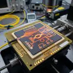
A $200 million price tag and room-sized footprint have long restricted access to extreme ultraviolet (EUV) lithography, a crucial technology for manufacturing modern electronics; however, engineers at the Cockrell School of Engineering have developed a tabletop EUV printer that lowers the barrier to semiconductor research. This new device is paired with a technique called volumetric 3D patterning, overcoming a significant limitation of current commercial EUV lithography which builds 3D nanostructures layer by layer, a process that can take days. “The actual printing might not take very long,” said Chih-Hao Chang, a professor in the Walker Department of Mechanical Engineering, “But the processing can take days.” By enabling parallel printing of multiple layers, the team’s method reduces exposure times to minutes, potentially accelerating innovation in fields ranging from computer chips to nanodrugs and quantum computing. The research, detailed in Nano Letters, was supported by the National Science Foundation Future of Semiconductors competition.
Table-Top EUV Lithography Device Reduces Semiconductor Manufacturing Costs
This new table-top system achieves comparable resolution by focusing on core components, offering increased versatility and modularity for researchers eager to explore advanced chip designs. The team’s innovation extends beyond the hardware, pairing the compact printer with volumetric 3D patterning, addressing a critical limitation of current EUV processes. Currently, the device is limited to patterning periodic structures, making it well-suited for applications in memory chips and photonics, but the team is actively testing new EUV materials developed in collaboration with UT Dallas and Johns Hopkins University. Saurav Mohanty, a recent Ph. D. graduate student and the study’s first author, said the ability to pattern 3D nanostructures could find applications in medicine for nanodrugs, quantum computing, or synthesizing novel materials, hinting at a broad range of potential future applications.
Volumetric 3D Patterning Enables Parallel Nanostructure Printing
The established process of extreme ultraviolet (EUV) lithography, essential for fabricating modern semiconductor chips, traditionally builds three-dimensional nanostructures layer by layer, a method that can extend processing times to days despite relatively swift initial printing. This innovation pairs with a newly developed tabletop EUV lithography device, a significant departure from the room-sized, over $200 million machines currently used in commercial semiconductor manufacturing. The team’s system achieves accelerated processing times, reducing exposure durations from days to minutes, by focusing on core components and streamlining the printing process. Currently, the technique is best suited for creating periodic structures, proving useful in the development of memory chips and photonic devices; however, the long-term vision extends to fabricating increasingly complex features for even smaller semiconductor switches. Saurav Mohanty, a recent Ph. D.
“Beyond semiconductor manufacturing, the ability to pattern 3D nanostructures can find applications in medicine for nanodrugs, quantum computing or synthesizing novel materials,”



See today’s quantum computing news on Quantum Zeitgeist for the latest breakthroughs in qubits, hardware, algorithms, and industry deals.