

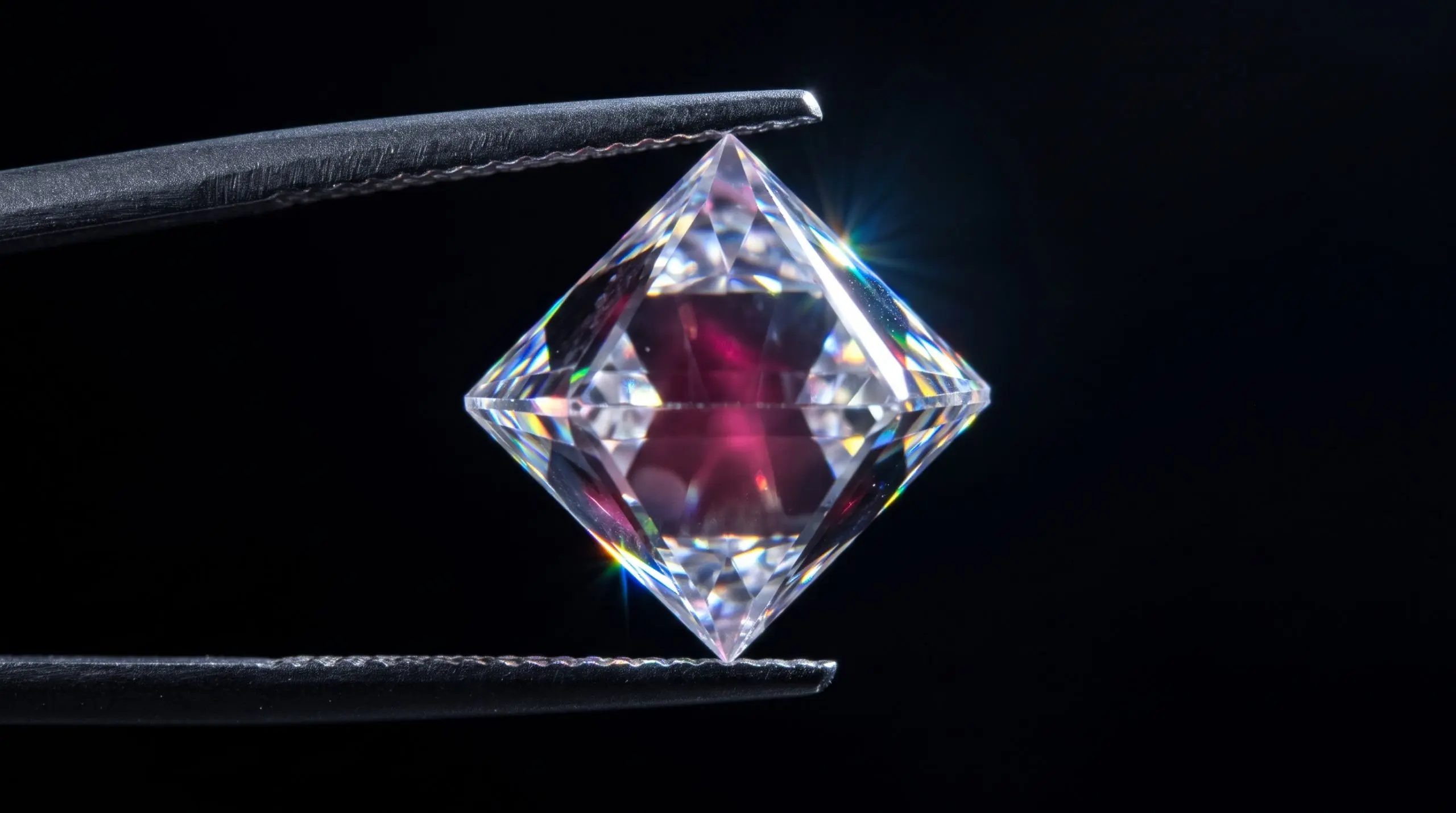
FBH achieves a remarkably smooth foundation for quantum devices, reporting surface roughness of just 0.5 nm rms after plasma etching. This level of precision eliminates mechanical polishing strain and surface damage, critical for minimizing interference in delicate quantum systems.
The company’s process removes up to 20 µm of material using oxygen- and chlorine-based plasma etching, and allows for the precise implantation of carbon, nitrogen, silicon, germanium and tin into diamond substrates to create efficient quantum memories and sensors. Backed by research through its Joint Lab Diamond Nanophotonics with Humboldt Universität zu Berlin, FBH offers scalable processes to advance quantum technology development.
Plasma Etching Removes Strain and Damage
This process creates a well-defined, low-damage foundation with a measured surface roughness of just 0. The technique avoids the introduction of defects that compromise the coherence of quantum states within the diamond. These implanted elements create color centers, which function as efficient quantum memories and sensors, tailoring the diamond’s properties for specific applications. This controlled implantation allows for the creation of low-noise, high-coherence centers essential for reliable quantum information processing.
Researchers can select individual steps or commission a complete fabrication workflow, integrating established and emerging color centers into photonic systems for quantum communication and sensing applications. The company’s platform is a toolbox for building bright, compact quantum light sources and high-sensitivity diamond-based sensors.




See today’s quantum computing news on Quantum Zeitgeist for the latest breakthroughs in qubits, hardware, algorithms, and industry deals.