
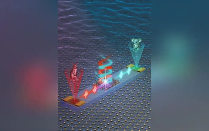
Monash University researchers have created the first fully integrated nanoscale circuit capable of generating, directing, and reading light-based information all on a single chip, a development that could advance quantum and artificial intelligence technologies. The new system harnesses the “valley degree of freedom,” a quantum characteristic of materials, to encode and process data in a potentially faster and more energy-efficient manner. This breakthrough overcomes a key limitation in the emerging field of valleytronics, which previously required separate components for signal generation and detection. “Until now, we could generate or detect these signals, but not do everything in one integrated device,” said lead author Dr. Chi Li, whose study appears in Nature Photonics. The device operates at room temperature and demonstrates the ability to simultaneously process multiple data streams, enabling compact, programmable photonic devices and scalable chip-based technologies.
Photonic Valleytronics Chip Integrates Light and Quantum Materials
Researchers at Monash University have achieved full integration of light-based information processing onto a single nanoscale chip, a development that could accelerate advancements in both quantum computing and artificial intelligence. The team successfully combined ultrathin materials with meticulously designed nanostructures to overcome a longstanding obstacle in the field of valleytronics; previously, scientists could either generate or detect signals leveraging the “valley degree of freedom,” but not perform both functions on a single platform. This new system utilizes a stacking approach, integrating materials and metasurfaces to bypass the difficulties of directly growing materials onto photonic structures, allowing for further innovation. The device operates at room temperature, a critical advantage over many quantum technologies that demand costly and complex cryogenic cooling systems, significantly broadening its potential for practical deployment. Dr. Chi Li, lead author of the study, said the breakthrough solves a key bottleneck that has limited the field for years.
Room-Temperature Nanoscale Circuit Enables On-Chip Information Processing
Unlike previous approaches that could only achieve signal generation or detection, this system performs all functions within a compact device, representing a significant step toward practical applications. Dr. Xing, co-first author and Research Fellow at Monash University, explained the fabrication process, stating, “We employ a stacking approach to integrate ultrathin materials with metasurfaces, overcoming the technical challenges of direct material growth on photonic structures and enabling further advances in valleytronics.” The device relies on materials only a few atoms thick, meticulously engineered with nanostructures to precisely control light behavior at minuscule scales, allowing for the encoding and processing of data in novel ways. This operating condition expands the potential for widespread adoption and integration into existing technological frameworks.
Senior author Dr. Haoran Ren, ARC Future Fellow and leader of Monash NanoMeta Group, believes this work opens the door to a new class of compact, programmable photonic devices, with potential applications spanning quantum computing, advanced imaging, and next-generation optical communication systems. Professor Stefan A. Maier, Head of the School of Physics and Astronomy and Nanophotonics Laboratory at Monash, added that by combining light and quantum materials on a chip, researchers can access new ways of encoding and processing information.
We employ a straightforward stacking approach to integrate ultrathin materials with metasurfaces, overcoming the technical challenges of direct material growth on photonic structures and enabling further advances in valleytronics.
Dr Xing, co-first author and Research Fellow at Monash University




See today’s quantum computing news on Quantum Zeitgeist for the latest breakthroughs in qubits, hardware, algorithms, and industry deals.