

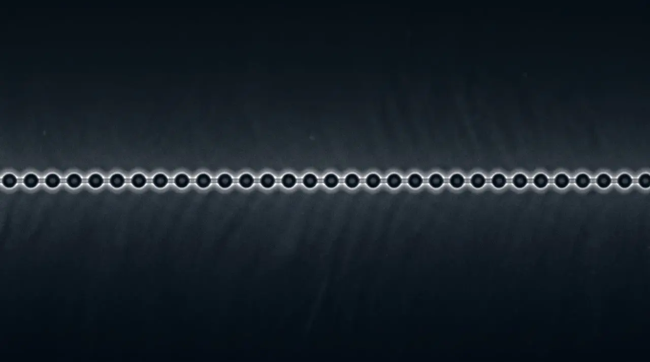
Researchers have created an air-stable superconductor only one or a few atoms thick, overcoming a major hurdle in the development of scalable quantum technologies. The team “grew” niobium diselenide underneath a protective layer of carbon-based graphene, preventing rapid degradation from oxidation while enabling large-scale production.
This advance allowed them to successfully integrate the material into a superconducting microwave circuit, demonstrating high kinetic inductance essential for many quantum devices. “Emerging superconductors that are only a monolayer thick have a lot of potential,” says Xudong Sheldon Zheng, a graduate student at MIT’s Department of Electrical Engineering and Computer Science; “Thanks to our new process, they are no longer materials that can only be made at a very small scale.”
Graphene-Protected Growth Enables Air-Stable Niobium Diselenide
The resulting niobium diselenide film, grown within a gap of less than one nanometer, exhibits exceptional stability in air; previously, such ultrathin superconductors degraded rapidly upon exposure to the environment. This encapsulation prevents oxidation, a common issue that typically damages the material after removal from its protective growth environment, according to the research team. A key element of their success lies in the precise control over growth conditions, allowing for tailored material formation between the graphene and silicon dioxide layers.
“By carefully tuning the growth conditions, we can ensure the material grows between the layers in exactly the way we’ve designed,” explains Xudong Sheldon Zheng. Weak adhesion between graphene and silicon dioxide creates a confined space for crystal formation, enabling the creation of a continuous monolayer exceeding one inch in size.
This approach differs from simply coating the material, as the niobium diselenide is grown underneath the graphene, a critical detail for maintaining its properties. The resulting air-stable film offers significant advantages for quantum device fabrication, particularly in applications requiring large kinetic inductance. Integrating this material into circuits could replace arrays of Josephson junctions with a compact thin-film alternative, reducing circuit size and complexity.
Addressing a key challenge in working with such thin materials, connecting them to electrodes, remains an area of focus; the material’s one-nanometer thickness presents difficulties in establishing reliable electrical contact. The team acknowledges this challenge while also noting that they are making progress.
It took a long time for us to understand how the growth could happen underneath the graphene. Through collaboration and discussion, we eventually uncovered the mechanism for growing the material at the interface, and this solves a lot of problems and allows us to simplify our fabrication steps.
Xudong Sheldon Zheng, a graduate student in the MIT Department of Electrical Engineering and Computer Science (EECS)
Niobium Diselenide Exhibits High Kinetic Inductance for Quantum Devices
The high kinetic inductance of niobium diselenide directly addresses a key challenge in quantum circuit design; the material stores a substantial amount of inductive energy within a remarkably small area, a characteristic previously difficult to achieve. Large kinetic inductance is a desirable trait, and conventionally realized through arrays of Josephson junctions, but integrating this thin-film material offers a path toward significantly more compact circuits. When incorporated into a superconducting circuit, the fabricated niobium diselenide maintained its superconducting properties and exhibited the expected high kinetic inductance, demonstrating functionality beyond initial material creation.
This successful integration represents a departure from previous limitations, as the team reports demonstrating a reliable electrical connection within a conventional circuit. The demonstrated growth strategy extends beyond niobium diselenide, potentially enabling the fabrication of a wider range of monolayer quantum materials with diverse properties. Beyond the immediate benefits for circuit miniaturization, the researchers are already looking ahead to future work.
It is challenging to make a good electrical connection between this very thin material, which is only about 1 nanometer in thickness, and our electrodes, which are a few hundred nanometers in thickness.
Sameia Zaman SM ’24, an EECS graduate student
Wafer-Scale Fabrication Overcomes Degradation Challenges
The fabrication process relies on a precise layering technique, beginning with graphene deposited onto a silicon dioxide substrate; this initial step creates a nanoscale gap essential for subsequent growth. Researchers then introduce precursor materials into this space, fostering the formation of niobium diselenide exclusively within the sub-nanometer void between graphene and the substrate. This method circumvents a longstanding issue with monolayer superconductors. Successfully growing the superconductor underneath graphene, rather than on an exposed surface, proved challenging, requiring significant collaborative effort to understand the underlying mechanisms.
“It took a long time for us to understand how the growth could happen underneath the graphene. Through collaboration and discussion, we eventually uncovered the mechanism for growing the material at the interface, and this solves a lot of problems and allows us to simplify our fabrication steps,” Zheng says, highlighting the importance of interdisciplinary teamwork in overcoming this hurdle.
The resulting graphene-niobium diselenide structure can then be safely transferred to ambient conditions without immediate degradation, a critical step toward practical applications. This approach extends beyond simply protecting the material; it enables wafer-scale fabrication, moving beyond the limitations of small-scale production. The team also refined an oxidation-free transfer technique, building on previous work to peel the composite structure from its growth substrate.
Emerging superconductors that are only a monolayer thick have a lot of potential. Thanks to our new process, they are no longer materials that can only be made at a very small scale. There are now exciting opportunities for scientists to study these materials, utilize them in circuits, and explore their practical applications.
Underlayer Technique Facilitates Monolayer Uniformity & Transfer
The fabrication process yielded niobium diselenide layers exceeding one inch in size, a scale previously unattainable for this class of superconductor due to environmental instability. This level of control stems from the deliberate creation of a sub-nanometer gap between graphene and silicon dioxide, confining the precursor materials and directing crystal formation. The resulting structure isn’t merely stable, but also facilitates a streamlined transfer process, building upon the team’s earlier oxidation-free techniques for peeling the composite material from its growth substrate.
Successfully isolating the superconductor beneath graphene addresses a critical challenge in connecting these ultrathin films to conventional circuitry. Wafer-scale production, now enabled by this underlayer technique, opens avenues for broader applications beyond fundamental research. The team anticipates further exploration of both the physics and potential uses of this material, envisioning a future with more scalable quantum devices.
By carefully tuning the growth conditions, we can ensure the material grows between the layers in exactly the way we’ve designed.
Xudong Sheldon Zheng, a graduate student in the MIT Department of Electrical Engineering and Computer Science (EECS)



See today’s quantum computing news on Quantum Zeitgeist for the latest breakthroughs in qubits, hardware, algorithms, and industry deals.