
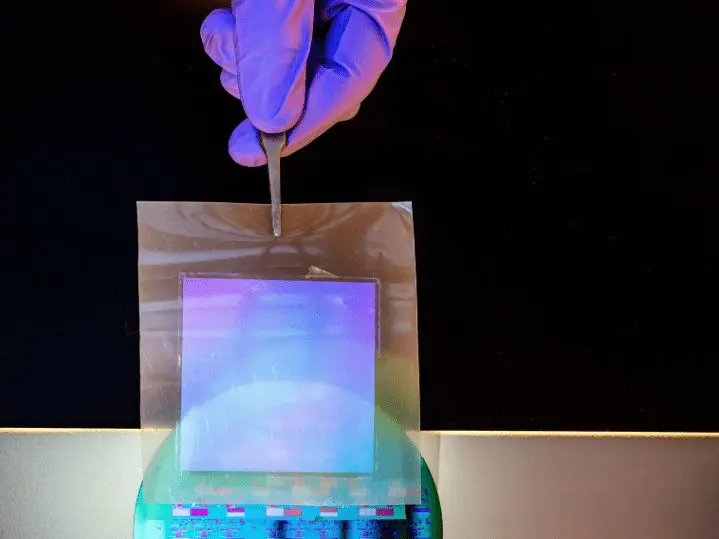
Researchers led by Qing Cao of Illinois Grainger Engineering have achieved an advance in chip design, demonstrating a scalable method for directly stacking high-performance silicon circuits. This breakthrough addresses a fundamental limitation in modern computing: the physical constraints of shrinking transistors on traditional, flat chips. The team’s process allows for the creation of three-dimensional chips, potentially extending Moore’s law by increasing density and speed while reducing energy consumption. “Today it takes six microelectronic devices called transistors on a single plane to store one bit of information,” explains Associate Professor Qing Cao, Department of Materials Science and Engineering; “With vertical integration, you can distribute them across multiple layers.” This newly invented process, detailed in Nature, utilizes standard single-crystalline silicon and achieved device yields of 98, 100%, signaling a viable path toward widespread industrial adoption of monolithic 3D integration.
Sequential Stacking of Silicon Extends Moore’s Law
Six transistors currently represent the storage capacity of one bit of information on a single plane, a density that researchers at Illinois Grainger Engineering are actively challenging through a novel approach to chip construction. For over half a century, computational power has advanced by relentlessly shrinking transistor size and increasing their density on flat chips; however, devices are now approaching atomic dimensions, where quantum effects and material properties impose fundamental constraints. Cao’s team addresses this challenge by building upwards, creating three-dimensional chips that dramatically increase computing density and speed while simultaneously reducing energy consumption. This isn’t simply about layering existing chips; the Illinois Grainger Engineering approach focuses on monolithic three-dimensional integration, where each layer is directly built upon the previous one to maximize connectivity.
Achieving this has long been a technical hurdle, primarily due to the extreme temperatures required for silicon processing, which would destroy the metal wiring in subsequent layers. “Generally, the industry accepts that once the first layer of circuits is complete, the thermal budget limit for any additional layers is 400 degrees Celsius,” Cao said, outlining the strict temperature constraints. The team circumvented this limitation by utilizing freestanding sheets of single-crystalline silicon, transferred onto a silicon wafer already patterned with the first layer of circuits. This innovative process maintains high device performance across multiple tiers while remaining within the critical 400-degree Celsius thermal budget. Crucially, the process has demonstrated device yields of 98, 100%, even within an academic laboratory setting, suggesting a strong potential for industrial scalability.
A roll laminator enables uniform stacking of these layers, allowing for precise alignment and minimizing defects. This advance has particularly significant implications for static random-access memory (SRAM), a ubiquitous component in central processing units and graphics processing units. Cao explained that static random-access memory is universal in CPUs and GPUs, and that this technology is like replacing a sprawling suburb with high-rises: you get the same functionality, but the spatial footprint is reduced while making communication between layers faster and more efficient. While vertical integration is already appearing in specialized AI hardware, Cao believes monolithic integration “unlocks the full promise of 3D chips,” adding, “For the first time, we have met the thermal budget of monolithic 3D integration using standard single-crystalline silicon and delivered improved performance.” The research, published in Nature, is being conducted within the Center for Advanced Semiconductor Chips with Accelerated Performance, which includes industry partners like IBM, Intel, and the Taiwan Semiconductor Manufacturing Company, and the team is now preparing to translate their process to an industrial semiconductor foundry.
Monolithic 3D Integration Overcomes Thermal Constraints
The pursuit of ever-increasing computing power has long relied on shrinking transistor sizes and packing them more densely onto silicon chips; however, this conventional approach is nearing fundamental physical limits imposed by atomic dimensions and quantum effects. While the industry explores novel materials, a compelling alternative, building upwards through three-dimensional integration, is gaining traction, promising to extend Moore’s law without necessarily reducing transistor scale. Current commercial 3D chips typically bond pre-fabricated wafers together, a method that introduces limitations in alignment and interlayer connectivity. Consequently, the thermal budget for each additional layer is strictly limited to 400 degrees Celsius. This innovative method allows for sequential stacking while staying within that limit, preserving the integrity of underlying metal interconnects. Alternatives to single-crystalline silicon, such as polycrystalline silicon or nanomaterials, have been explored, but these often compromise device performance and reliability due to material defects or intrinsic limitations. The Illinois Grainger Engineering team’s method avoids these issues by continuing to utilize standard single-crystal silicon, ensuring compatibility with existing manufacturing infrastructure.
Vertical integration is already starting to make its way into commercial devices, particularly in specialized AI hardware, but monolithic integration is what unlocks the full promise of 3D chips.
Single-Crystalline Silicon Achieves 98-100% Device Yields
Qing Cao, a professor at Illinois Grainger Engineering, is spearheading a new approach to chip fabrication that directly addresses the limitations of conventional scaling. Cao’s team has successfully demonstrated a method for sequentially stacking high-performance silicon circuits, achieving device yields of 98, 100%, a figure previously unattainable in academic settings and indicative of potential for industrial scalability. The research, recently published in Nature, details a process that maintains high device performance across multiple stacked layers of silicon, a critical step towards realizing fully three-dimensional chips. The core challenge in monolithic three-dimensional integration lies in the thermal budget. Cao’s team circumvented this by staying within a thermal budget limited to 400 degrees Celsius. A roll laminator enables uniform stacking, allowing for sequential layering without compromising the integrity of the underlying structures. This innovation directly addresses a fundamental shift in how computing density is achieved.
This is akin to replacing a sprawling suburban landscape with high-rise buildings, achieving the same functionality in a significantly smaller space. The high device yields suggest a viable path towards commercialization.
Generally, the industry accepts that once the first layer of circuits is complete, the thermal budget limit for any additional layers is 400 degrees Celsius.
Vertical Integration Enhances AI and Data-Intensive Computing
The demand for ever-increasing computational power is driving materials scientists to explore new approaches to chip design, and a recent advance from the Illinois Grainger Engineering department offers a pathway beyond traditional scaling limitations. The conventional approach to boosting processing power, shrinking transistors, is rapidly approaching fundamental physical limits. As devices become increasingly miniaturized, quantum effects and atomic dimensions present obstacles. This sequential stacking, known as monolithic three-dimensional integration, offers significant advantages over existing 3D chip manufacturing methods. Monolithic integration builds each layer directly onto the previous one, enabling denser connections and nanometer-scale precision. The key breakthrough lies in overcoming the thermal constraints inherent in this process. Traditional silicon fabrication requires temperatures exceeding 1,000 degrees Celsius, which would destroy existing metal wiring on lower layers, so the thermal budget is strictly set to 400 degrees for upper layers beyond the first. The resulting devices have demonstrated impressive yields of 98, 100%, setting a new standard and suggesting strong potential for industrial scalability.
For the first time, we have met the thermal budget of monolithic 3D integration using standard single-crystalline silicon and delivered unprecedented performance.



See today’s quantum computing news on Quantum Zeitgeist for the latest breakthroughs in qubits, hardware, algorithms, and industry deals.