


Wenjun Zheng and colleagues have demonstrated real-space manipulation of micrometer-scale incompressible strips within graphene, creating tunable topological boundaries. The work establishes these strips, formed by controlling carrier density and magnetic field in graphene placed on a SrTiO₃ substrate, as a platform for exploring internal quantum Hall boundaries. This high-dielectric substrate widens the typically nanoscale region to a visible scale, allowing direct probing of charge inhomogeneity and quantum Hall physics across the entire device. These results suggest potential utility as dynamically reconfigurable channels for topological charge transport.
Graphene Quantum Hall Boundaries on Dielectric Substrates
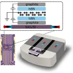
Graphene placed on a strontium titanate (SrTiO₃) substrate enables the creation of incompressible strips induced by charge gradients within the quantum Hall regime. This configuration allows for efficient electrostatic doping due to the substrate’s high dielectric constant, a property critical for manipulating carrier density within the graphene. The use of a 500-micrometer-thick SrTiO₃ layer, however, introduces fringing fields that significantly affect electrostatic doping, particularly when the graphene sample is smaller than the underlying gate.
The resulting manipulation of carrier density manifests as higher concentrations and stronger polaritonic signals on the hole-doped side of the graphene when a negative gate voltage is applied. Researchers observed a minimum in the phase velocity at the charge neutrality point, a phenomenon linked to the formation of these internal quantum Hall boundaries.
Hysteresis behavior in both phase velocity and carrier density, previously observed in graphene devices on high-κ substrates, arises from variations in the dielectric environment beneath the graphene. This behavior, documented in figures within the study, highlights the sensitivity of the system to subtle changes in the substrate. To fully characterize these boundaries, Wenjun Zheng and colleagues employed a combination of space and time-resolved terahertz nanoscopy alongside infrared nearfield photocurrent imaging.
This multimodal approach allowed for detailed mapping and tracking of the quantum Hall boundaries within the graphene, providing a robust method for analyzing their behavior in studies of photo-thermoelectric effects at graphene interfaces. This reconfigurability, achieved through precise control of electrostatic doping, opens possibilities for novel electronic devices that use the unique properties of quantum Hall systems. Dai, Zheng, Jing, and colleagues published their findings in Light: Science & Applications in 2026, detailing the methods used to visualize and manipulate these internal boundaries.
SrTiO₃ Substrate Enhances Incompressible Strip Width
Researchers used space and time-resolved terahertz nanoscopy to map carrier density gradients within the graphene, providing a detailed view of these quantum phenomena. To fully characterize the location and behavior of these incompressible strips, the team employed a dual imaging approach, combining terahertz nanoscopy with infrared nearfield photocurrent imaging. This multimodal technique allowed for the extraction of local plasmon phase velocities, offering a quantitative measurement of carrier density variations throughout the graphene sample.
The resulting data confirmed the formation and spatial manipulation of the incompressible strip, demonstrating a method for controlling it through electrostatic gating. The ability to manipulate these boundaries through adjustments to both magnetic field and carrier density opens possibilities for novel electronic devices and a deeper exploration of topological charge transport.
Terahertz Nanoscopy Maps Charge Density Gradients
The width of incompressible regions, acting as topological boundaries within graphene, can be calculated using a formula incorporating the effective dielectric function of the graphene environment, energy gaps between Landau levels and the carrier density gradient. This approach allowed for visualization of quantum Hall boundaries separating areas with differing sub-Landau level occupations, boundaries manipulated by adjusting both magnetic field strength and carrier density.
Z.D. and J.P. performed the terahertz scattering-type scanning near-field optical microscopy, while W.Z., Z.D., and L.W. conducted the infrared photocurrent nanoscopy experiments, establishing a robust method for probing these quantum phenomena. Theoretical calculations, performed by Z.D., R.J., and M.F., support the observed behavior and provide quantitative insight into the underlying physics.
The calculated width of these incompressible strips depends on the dielectric properties of the surrounding materials, specifically the hexagonal boron nitride encapsulating the graphene and the strontium titanate substrate itself. “w^{2}=/{2κ Δ {E}_{LL^{′ }}}{π ^{2}{e}^{2}{dn}/dx},” the paper states, detailing the equation used to determine strip width based on these parameters.
Fabrication of the devices and transport measurements were conducted by B.Z. and L.W., while M.L., R.J., and L.W. Numerical simulations, carried out by X.C. and R.J., further validated the experimental findings. All coauthors contributed to the data analysis.
Infrared Photocurrent Imaging Tracks Boundary Location
Infrared photocurrent nanoscopy directly visualizes the location of incompressible strips within graphene, revealing shifts in their boundaries with applied magnetic fields. The use of a strontium titanate substrate broadened the observable region to micrometer scale, facilitating direct observation of the interplay between charge distribution, electrostatic shielding and quantum Hall physics.
The location of these incompressible boundaries demonstrably changes with increasing magnetic field strength, as observed through photocurrent generation. The team’s work, which included device fabrication and transport measurements by B.Z. and L.W., further solidifies the method’s robustness for investigating these quantum systems and opens avenues for future exploration of reconfigurable electronic components.
Landau Level Quantization and Compressible Strips
The interplay of Landau level quantization and electrostatic screening within graphene creates alternating compressible and incompressible strips, even deep within the material itself, particularly when a significant doping gradient exists. This spontaneous formation of these regions is driven by the unique properties of graphene placed on a strontium titanate substrate, which shapes the electron density distribution.
The strong dielectric screening provided by the substrate, combined with inherent device asymmetry, establishes the necessary charge gradient for these strips to emerge. The location of these boundaries is not fixed; adjusting the back-gate voltage shifts the chemical potential relative to the Landau levels, directly causing the incompressible boundary to move.
This tunability is a key feature, as it demonstrates a method for controlling the electronic properties within the graphene itself. Simulations reveal that a tilting of Landau levels forms compressible regions corresponding to partially filled levels, separated by the incompressible strip. The microscopic structure of quantum Hall edge states can vary, but this work highlights how these boundaries can be visualized and manipulated.
A schematic illustration shows that when the Fermi level crosses a Landau level, a compressible region forms, delineated by an incompressible area emerging due to Landau level energy transitions. Researchers used a combination of techniques to map these boundaries, including terahertz nanoscopy and near-field photocurrent imaging, to observe the behavior of plasmon polaritons propagating toward the graphene edges.
Internal Boundaries Enable Reconfigurable Topological States
Internal quantum Hall boundaries within graphene exhibit a degree of control previously unseen, with their location tunable through external manipulation. This technique, combined with space and time-resolved terahertz nanoscopy, provides a robust method for characterizing these quantum Hall boundaries and their response to external stimuli.
“Controlling internal boundaries in quantum Hall systems offers a route to engineering reconfigurable topological states,” the researchers write, highlighting the potential for creating novel electronic devices. The ability to manipulate these boundaries opens avenues for exploring fundamental physics and designing systems with tailored topological properties, potentially leading to advancements in areas like quantum computing and spintronics.
THz s-SNOM Visualizes Plasmon Polariton Phase Velocities
Terahertz spacetime mapping directly quantified plasmon phase velocities within graphene, revealing a correlation to local carrier density variations across the material. The technique, detailed in recent work, relies on a strontium titanate substrate to enhance the width of incompressible regions, areas where electron movement is restricted due to quantum effects, allowing for visualization at a scale exceeding typical nanoscale limitations. This broadened region facilitated the extraction of phase velocity data using nano-THz imaging, providing a quantitative measure of charge distribution.
The observed behavior of chiral photocurrents aligned with experimental results, confirming the link between carrier density and plasmon propagation. Researchers demonstrated control over the system through electrostatic gating, visualizing these states with near-field probes. By combining terahertz spacetime mapping with infrared photocurrent imaging, the team spatially manipulated an incompressible strip within the graphene, demonstrating a dynamically reconfigurable channel for charge transport.
The calculated phase velocity at a fixed frequency accurately approximated velocities across a broad 0.5-1.5 THz spectrum, a characteristic of acoustic graphene plasmons. “By combining THz space-time polariton imaging and IR PCN, we observed the formation and spatial manipulation of an incompressible strip in graphene on a high-dielectric SrTiO₃ substrate,” the researchers report, highlighting the effective combination of the two imaging modalities. The resulting data supports the understanding of how electrostatic potential influences carrier density and, consequently, the behavior of plasmon polaritons within the graphene structure.
Electrostatically Induced Charge Gradients in Graphene
The high dielectric screening of SrTiO₃ enhances the width of the incompressible region to the micrometer scale, allowing direct probing of the interplay of charge inhomogeneity, electrostatic screening and quantum Hall physics across the entire device. This broadening stems from the use of a strontium titanate (SrTiO₃) substrate, which facilitates electrostatic doping due to its high dielectric constant. However, the substrate’s thickness, 500 micrometers and the graphene sample’s comparatively small size introduce fringing fields that notably influence electrostatic doping.
Researchers found that variations in local carrier densities, estimated at 0.6 x 1012 cm-2 on the top side and 0.15 x 1012 cm-2 on the bottom near the charge neutrality point, contribute to these gradients. These inhomogeneities may arise from edge fringe-field effects or local surface dipoles at the graphene-STO interface, influencing the distribution of charge carriers. Visualizing these boundaries relied on outlining graphene edges with green dash-dotted lines and mapping charge inhomogeneity boundaries with dotted lines.



See today’s quantum computing news on Quantum Zeitgeist for the latest breakthroughs in qubits, hardware, algorithms, and industry deals.