

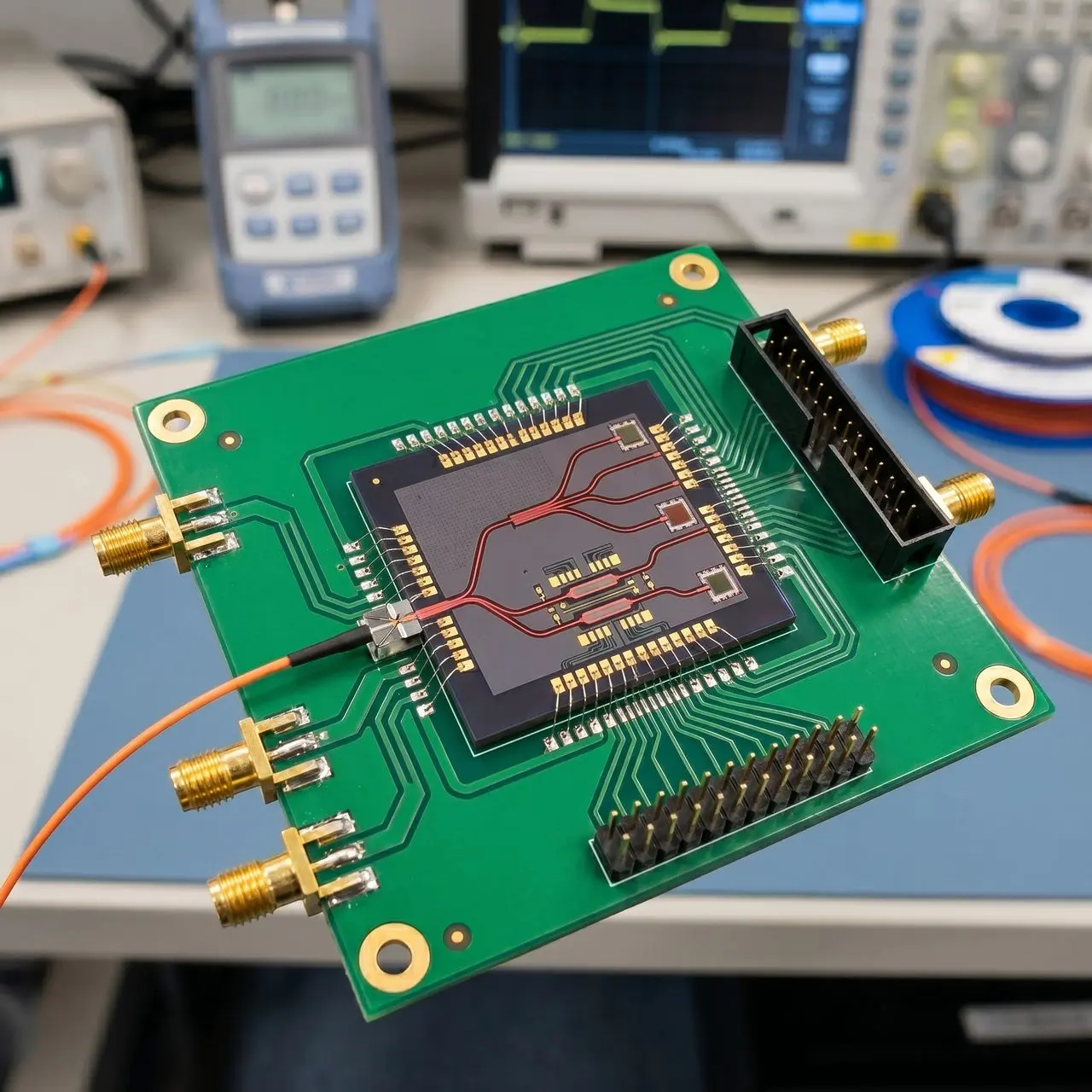
Researchers at the Max Planck Institute and Harvard’s John A. Paulson School of Engineering and Applied Sciences have created silicon nitride photonic components reduced in size by a factor of 500 compared to conventional designs. The team employed an inverse-design algorithm, first defining the desired light behavior and then allowing a computer to search for the precise nanostructures to achieve it. This approach yielded wavelength splitters, mode sorters, and mirrors, three functional components demonstrating broad applicability for denser, higher-performance integrated photonic circuits. “Inverse design becomes practical when fabrication realities are built into the optimization,” said Kiyoul Yang, co-lead author of the research, noting that the designs are compatible with commercial manufacturing processes. The resulting microchip, containing hundreds of these components, is visualized alongside a 10-euro-cent coin to illustrate the scale of miniaturization.
Inverse Design of Silicon Nitride Photonic Components
This miniaturization promises to dramatically increase the density and performance of integrated photonic circuits, essential for applications ranging from telecommunications to quantum computing. Conventional photonic chip design relies on iterative adjustments of established geometries; this new method reverses that process, beginning with a desired light behavior and computationally generating the optimal nanostructure. The team successfully created three key functional components, wavelength splitters, mode sorters, and mirrors, all benefiting from this substantial size reduction. The researchers demonstrated broad applicability of the inverse-design approach, and the algorithm incorporates minimum feature sizes and accounts for manufacturing variations, ensuring designs are both compact and commercially viable. Silicon nitride was chosen as the base material due to its low optical loss and ability to generate clean light across a spectrum of colors.
Previously, research focused on silicon, diamond, silicon carbide, and lithium niobate, but thick silicon nitride now offers a compelling alternative. The inverse-designed mirrors, measuring just micrometers across, achieve a remarkable 98.5% reflectivity while blocking unwanted spatial modes, and when paired, create optical cavities where light can bounce over 100 times before escaping. Toby Bi, co-lead author of the study and researcher at the Max Planck Institute, explains, “Inverse design lets us define what we want light to do, and the optimization finds a structure that does it, often one no human would have drawn.” The team intends to integrate these components with nonlinear optical circuits, potentially enabling advanced applications in precision measurement, telecommunications, and quantum technologies.
Thick silicon nitride underpins most of the high-performance integrated photonics we work with, but until now its component library was limited to hand-engineered designs.
Pascal Del’Haye, head of the microphotonics research group at Max Planck Institute
The current landscape of photonic microchip design traditionally relies on iterative refinement of established geometries, a process that limits both the speed of innovation and the ultimate density of integrated circuits. Researchers are now demonstrating that computer-driven inverse design offers a pathway to overcome these limitations, yielding components drastically smaller than those created through conventional methods. These newly designed components address critical needs within photonic circuits.
Inverse design becomes practical when fabrication realities are built into the optimization.
Kiyoul Yang, SEAS assistant professor of electrical engineering
Compact Designs Enable Integrated Quantum Photonic Circuits
Researchers are achieving significant miniaturization in photonic circuits, with implications for quantum technologies and beyond. Kiyoul Yang, assistant professor of electrical engineering at Harvard’s John A. Paulson School of Engineering and Applied Sciences, co-led the work with Pascal Del’Haye, head of the microphotonics research group at Max Planck Institute. This advance, published in Nature Communications, addresses a critical bottleneck in the development of faster, more efficient data processing systems. Rather than starting with a known shape and refining it, the algorithm searches a vast design space for nanostructures that fulfill specific optical functions. These resulting structures, often appearing as irregular patterns of holes and ridges, precisely manipulate light within an area smaller than the width of a human hair. These devices, showcased alongside a 10-euro-cent coin to illustrate their scale, are not merely smaller versions of existing technology; they represent a fundamentally new design paradigm.
Mirrors, measuring only a few micrometers across, reflect up to 98.5% of incoming light while blocking other spatial modes. When placed in pairs, they form on-chip optical cavities in which light bounces more than 100 times between the mirrors before escaping.
Inverse design lets us define what we want light to do, and the optimization finds a structure that does it, often one no human would have drawn.
Toby Bi, co-lead author of the study and researcher at the Max Planck Institute




See today’s quantum computing news on Quantum Zeitgeist for the latest breakthroughs in qubits, hardware, algorithms, and industry deals.