MIT researchers have developed a chip-based optical device capable of dynamically controlling incoming mid-infrared light, potentially leading to more precise thermal imaging, chemical sensing, and pollution monitoring. Each microscopic pixel of the device’s lens can independently control infrared light, allowing for focus changes without the need for moving parts, a key advancement for creating miniaturized and faster sensing systems. The system, detailed in a paper published in Nature Communications, was built using mostly conventional semiconductor manufacturing processes, suggesting a viable path toward industrial-scale implementation. “This could give us more information as we study space, or help with environmental protections where you want to monitor for specific compounds in the atmosphere,” explains first author Cosmin-Constantin Popescu PhD ’25, highlighting the broad range of potential applications for the technology.
Tunable Metasurfaces Enable Dynamic Infrared Light Control
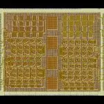
Each microscopic pixel within a newly developed chip-based device operates as an independent controller of infrared light, a capability that eliminates the need for mechanical movement to alter focus. This is a significant step toward miniaturization and increased operational speed. The system leverages metasurfaces, materials patterned with nanoscale precision, to manipulate light in ways conventional optics cannot. Unlike prior metasurface designs that adjusted focus across an entire material, this innovation allows for pixel-level control, addressing a key limitation in the field. “Most active metasurfaces trying to do single-pixel tuning need wires going to every pixel, and how you route the wires becomes a big issue,” explains Juejun Hu, MIT’s John F. Elliott Professor of Materials Science and Engineering. The team circumvented this challenge by adapting a crossbar architecture commonly used in display manufacturing, layering copper wires perpendicularly above a silicon layer that generates heat to switch the material’s phase.
This configuration, according to Hu, “allows us to scale to potentially millions of pixels without having any issues with unintended currents.” The researchers constructed a lab-scale demonstration utilizing largely conventional semiconductor manufacturing processes, a deliberate choice to facilitate industrial-scale implementation. This approach, they believe, will streamline the transition from prototype to practical application. The device operates in the mid-infrared wavelength, crucial for detecting heat signatures and molecules like methane and propane, with applications ranging from leak detection to atmospheric studies. The team demonstrated a 6-by-6 pixel array capable of reliable switching, with Popescu noting that the materials should switch a large number of times, perhaps tens of thousands of times or more, to be useful.
As you want to scale up, you need something that’s part of a consistent process, and that’s why chip foundry manufacturing becomes so important.
Juejun Hu, MIT’s John F. Elliott Professor of Materials Science and Engineering
Crossbar Architecture Achieves Pixel-Level Switching
The inclusion of a diode selector further prevents unwanted currents between pixels, a crucial element for scalability. “We found this mesh architecture to be very resilient,” says first author Cosmin-Constantin Popescu.
This could give us more information as we study space, or help with environmental protections where you want to monitor for specific compounds in the atmosphere.
Researchers at MIT are developing a new approach to infrared imaging with a chip-based device capable of dynamically controlling light at the microscopic level. The team, led by Juejun Hu, MIT’s John F. Elliott Professor of Materials Science and Engineering, has focused on a crossbar architecture borrowed from display manufacturing. Testing revealed a resilient system capable of repeated switching. The researchers are now focused on increasing pixel density and enhancing system robustness, paving the way for more sophisticated infrared sensing capabilities.
Basically, a lot of organic molecules absorb in the mid-infrared wavelength, and you could use this system to detect them.
The development of a scalable, chip-based infrared imaging system promises advancements beyond traditional thermal and chemical sensing, potentially impacting fields from space exploration to environmental monitoring. Researchers at MIT have demonstrated a device capable of dynamically controlling mid-infrared light, offering a pathway toward compact, tunable cameras and novel optical computing architectures. This innovation addresses a longstanding challenge; existing infrared systems are often bulky and expensive, limiting their widespread adoption. Each microscopic pixel within the new device independently manages infrared light, enabling focus adjustments without mechanical movement, a critical step for miniaturization and speed. This emphasis on established processes suggests a viable route toward industrial-scale production, moving beyond purely laboratory demonstrations. Central to the design is a crossbar architecture, adapted from display technology, featuring perpendicularly arranged copper wires atop a layer of doped silicon. Beyond imaging, the researchers envision applications in optical computing, where the metasurface could encode information for neural networks. “This could enable more effective optical computing, where metasurfaces are used to encode network weights in neural networks,” Hu explains, suggesting a future where light, rather than electricity, drives artificial intelligence.
In lots of cases when you’re taking images, you have prior knowledge of what you’re looking for.
Juejun Hu, MIT’s John F. Elliott Professor of Materials Science and Engineering



See today’s quantum computing news on Quantum Zeitgeist for the latest breakthroughs in qubits, hardware, algorithms, and industry deals.