
Magnetic Random Access Memory (MRAM) is an emerging technology that could revolutionize digital storage by offering a denser and more efficient solution. Despite challenges in developing MRAM, it remains a promising next-generation nonvolatile memory architecture. The technology is built around a magnetic tunnel junction (MTJ), which allows for high-speed read and write operations. Scanning NV magnetometry (SNVM), a non-contact metrology technique, is being used to investigate MRAM performance at the individual bit level. Quantum sensing is also being used to address metrology challenges, providing detailed insights into the magnetic properties of MRAM devices at the nanoscale.
What is the Significance of Magnetic Random Access Memory (MRAM)?
Magnetic Random Access Memory (MRAM) is an emerging memory technology that is set to replace current nonvolatile memory technologies such as eFlash. This technology is at a stage where controlling and improving the distribution of device properties is crucial for enabling new applications. MRAM’s significance lies in its potential to revolutionize the digital storage landscape by offering a more efficient and denser storage solution. As digital data continues to grow exponentially, the need for more efficient and compact storage solutions becomes increasingly important. MRAM, with its ability to store information magnetically, is poised to meet this demand.
The development of MRAM is not without its challenges. As magnetic bits become smaller and denser to improve storage density and energy efficiency, they present an ever-increasing challenge for metrology tools. This challenge is intensifying with the push towards exotic materials such as 2D and antiferromagnetic magnets, which have small surface moments. Despite these challenges, MRAM remains one of the most promising next-generation nonvolatile memory architectures, already in production for embedded flash replacement at N2X nodes.
MRAM is constructed around a magnetic tunnel junction (MTJ), a key component that contributes to its superior performance. The MTJ consists of two ferromagnetic layers separated by a thin insulating layer. When a voltage is applied across the layers, electrons can tunnel from one layer to the other, creating a magnetic field. This field can then be used to store information. The MTJ’s design allows for high-speed read and write operations, making MRAM a highly efficient memory technology.
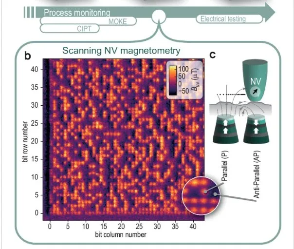
How Does Scanning NV Magnetometry (SNVM) Enhance MRAM Performance?
A non-contact metrology technique known as scanning NV magnetometry (SNVM) is introduced to investigate MRAM performance at the individual bit level. This technique allows for magnetic reversal characterization in individual 60 nm-sized bits to extract key magnetic properties, thermal stability, and switching statistics. By doing so, it can gauge bit-to-bit uniformity, a crucial factor in ensuring the reliable performance of MRAM devices.
SNVM offers several advantages over traditional metrology methods. Unlike ensemble averaging methods such as the perpendicular magneto-optical Kerr effect, SNVM can identify out-of-distribution tail-bits, bits that seem associated with the edges of the array. This ability enables failure analysis of tail bits, providing valuable insights into the performance and reliability of MRAM devices.
The use of SNVM in the investigation of MRAM performance showcases the potential of nanoscale quantum sensing of MRAM devices for early-stage screening in the processing line. This could pave the way for the future incorporation of this nanoscale characterization tool in the semiconductor industry, enhancing the production and performance of MRAM devices.
What is the Role of Quantum Sensing in MRAM Development?
Emerging ultrasensitive nanoscale magnetic quantum sensors offer a unique opportunity to address the metrology challenges presented by the development of MRAM. These sensors, due to their highly competitive sensing characteristics, can provide detailed insights into the magnetic properties of MRAM devices at the nanoscale. This capability is crucial for the development and optimization of MRAM technology.
Quantum sensing in an industrially relevant context and scale, such as in the case of spin transfer-torque magnetic random access memory (STT-MRAM), demonstrates the advantage of such quantum metrology. STT-MRAM is an ideal candidate for demonstrating the benefits of quantum sensing due to its status as one of the most promising next-generation nonvolatile memory architectures.
The findings from the use of quantum sensing in the investigation of MRAM performance highlight the potential of nanoscale quantum sensing of MRAM devices for early-stage screening in the processing line. This could pave the way for the future incorporation of this nanoscale characterization tool in the semiconductor industry, enhancing the production and performance of MRAM devices.
How Does MRAM Compare to Other Memory Technologies?
MRAM is set to replace current nonvolatile memory technologies such as eFlash. This is due to several advantages that MRAM offers over these existing technologies. For one, MRAM has the potential to offer higher storage density and energy efficiency. This is due to the use of magnetic bits, which can be made smaller and denser than the bits used in other memory technologies.
Furthermore, MRAM is constructed around a magnetic tunnel junction (MTJ), which allows for high-speed read and write operations. This makes MRAM a highly efficient memory technology, capable of meeting the increasing demand for fast and reliable digital storage.
However, the development of MRAM is not without its challenges. As magnetic bits become smaller and denser, they present an ever-increasing challenge for metrology tools. This challenge is intensifying with the push towards exotic materials such as 2D and antiferromagnetic magnets, which have small surface moments. Despite these challenges, MRAM remains one of the most promising next-generation nonvolatile memory architectures.
What are the Future Prospects for MRAM and Quantum Sensing?
The future of MRAM looks promising, with the technology poised to replace current nonvolatile memory technologies such as eFlash. The use of quantum sensing in the development and optimization of MRAM further enhances its prospects. Quantum sensing offers a unique opportunity to address the metrology challenges presented by the development of MRAM, providing detailed insights into the magnetic properties of MRAM devices at the nanoscale.
The findings from the use of quantum sensing in the investigation of MRAM performance highlight the potential of nanoscale quantum sensing of MRAM devices for early-stage screening in the processing line. This could pave the way for the future incorporation of this nanoscale characterization tool in the semiconductor industry, enhancing the production and performance of MRAM devices.
As the demand for more efficient and compact digital storage solutions continues to grow, the development and optimization of MRAM technology will become increasingly important. With the help of quantum sensing, the semiconductor industry can meet this demand, paving the way for a new era of digital storage.
What are the Implications of these Findings for the Semiconductor Industry?
The findings from the use of quantum sensing in the investigation of MRAM performance have significant implications for the semiconductor industry. They highlight the potential of nanoscale quantum sensing of MRAM devices for early-stage screening in the processing line. This could pave the way for the future incorporation of this nanoscale characterization tool in the semiconductor industry, enhancing the production and performance of MRAM devices.
The use of quantum sensing in the development and optimization of MRAM also offers a unique opportunity to address the metrology challenges presented by the development of MRAM. By providing detailed insights into the magnetic properties of MRAM devices at the nanoscale, quantum sensing can help the semiconductor industry overcome these challenges and optimize the performance of MRAM devices.
As the demand for more efficient and compact digital storage solutions continues to grow, the development and optimization of MRAM technology will become increasingly important for the semiconductor industry. With the help of quantum sensing, the industry can meet this demand, paving the way for a new era of digital storage.
Publication details: “A quantum sensing metrology for magnetic memories”
Publication Date: 2024-06-03
Authors: Vicent J. Borràs, Robert Carpenter, Liza Žaper, Siddharth Rao, et al.
Source: npj Spintronics
DOI: https://doi.org/10.1038/s44306-024-00016-5