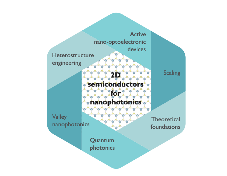
The manipulation of light at the nanoscale, a field known as nanophotonics, stands to revolutionise technologies ranging from optical computing to advanced sensing. Recent attention has focused on two-dimensional (2D) semiconductors, materials just a few atoms thick, as promising building blocks for these devices due to their unique optical properties and potential for integration. A collaborative effort involving researchers from numerous institutions now comprehensively assesses the current state and future direction of this rapidly evolving field. The perspective, entitled ‘Photonics in Flatland: Challenges and Opportunities for Nanophotonics with 2D Semiconductors’, is authored by Ali Azimi, Julien Barrier, Angela Barreda, Thomas Bauer, Farzaneh Bouzari, Abel Brokkelkamp, Francesco Buatier de Mongeot, Timothy Parsons, Peter Christianen, Sonia Conesa-Boj, Alberto G. Curto, Suprova Das, Bernardo Dias, Itai Epstein, Zlata Fedorova, F. Javier García de Abajo, Ilya Goykhman, Lara Greten, Johanna Grönqvist, Ludovica Guarneri, Yujie Guo, Tom Hoekstra, Xuerong Hu, Benjamin Laudert, Jason Lynch, Sabrina Meyer, Battulga Munkhbat, Dragomir Neshev, Masha Ogienko, Sotirios Papadopoulos, Aparna Parappurath, Jeroen Sangers, Pedro Soubelet, Chris Soukaras, Giancarlo Soavi, Isabelle Staude, Zhipei Sun, Klaas-Jan Tielrooij, MD Gius Uddin, Alexey Ustinov, and Jorik van de Groep. The work details both the considerable progress made in utilising these materials for active optical control and the remaining hurdles to scalable device fabrication and performance optimisation.
Research into two-dimensional (2D) materials is continuing to progress, with a focus on their potential applications in next-generation electronics and optoelectronics. A central theme involves achieving wafer-scale integration, the reproducible transfer of these materials from their growth substrate to the target substrate upon which devices are fabricated. Techniques such as adhesion lithography and wafer bonding are employed, though maintaining material integrity during transfer presents a significant challenge, as defects invariably degrade performance.
Improving charge transport and minimising contact resistance are also critical areas of investigation. High contact resistance impedes efficient current flow and diminishes device performance, therefore research concentrates on optimising interfaces between 2D materials and metallic contacts. For example, graphene-based contacts on molybdenum disulphide (MoS₂) field-effect transistors are being explored to maximise current flow and reduce energy loss.
Material and device optimisation remains a core focus,
Material and device optimisation remains a core focus, with researchers investigating novel materials combinations and device architectures to overcome inherent limitations. Heterostructure engineering, the layering of different 2D materials, allows for the tailoring of electronic and optical properties, expanding the range of potential applications. This approach enables the creation of materials with functionalities not present in single-layer materials.
Advanced characterisation techniques, coupled with computational modelling, are essential for understanding and mitigating sources of variability in material properties and device performance. Techniques such as Raman spectroscopy, atomic force microscopy and transmission electron microscopy provide detailed information about material structure and composition. Computational modelling allows researchers to predict material behaviour and optimise device designs. Chemical vapour deposition (CVD) remains a prominent technique for the scalable growth of 2D materials.
Investigations into the optical properties of these heterostructures reveal promising avenues for light harvesting. Nanorippled MoS₂ films, for instance, exhibit enhanced broadband light absorption, potentially improving the efficiency of solar cells and photodetectors. Furthermore, understanding fundamental phenomena such as exciton behaviour – bound electron-hole pairs – in 2D semiconductors on metal substrates is crucial for controlling light-matter interactions and developing novel optoelectronic devices.
Addressing long-term stability and reliability is paramount for the practical implementation of 2D material-based technology. Assessing yield, variability, and degradation mechanisms ensures the production of robust and dependable electronic components. Scalability and cost-effectiveness remain key challenges, hindering widespread adoption. Developing fabrication processes that are both efficient and economically viable is crucial for translating laboratory research into commercial products. Mitigating variability across entire wafers, ensuring consistent material quality and device performance, is also a significant hurdle.
👉 More information🗞Photonics in Flatland: Challenges and Opportunities
🗞 Photonics in Flatland: Challenges and Opportunities for Nanophotonics with 2D Semiconductors
🧠 DOI: https://doi.org/10.48550/arXiv.2507.00336


