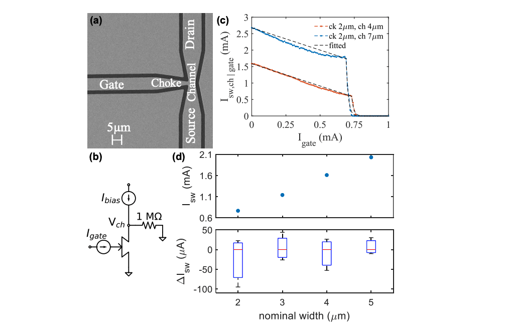
On April 22, 2025, researchers Dip Joti Paul, Tony X. Zhou, and Karl K. Berggren published Photolithography-Compatible Three-Terminal Superconducting Switch for Driving CMOS Loads, detailing a novel superconducting switch designed to interface with Complementary Metal-Oxide-Semiconductor (CMOS) electronics. This advancement addresses the need for cryo-electronics compatible with existing semiconductor technologies, enabling applications in ultra-low-power computing and next-generation electronic systems.
Researchers developed a three-terminal superconducting switch called wTron, fabricated using photolithography, enabling direct interface with CMOS electronics. The micron-width wire-based device exhibits output impedance over 1 kΩ and reduced sensitivity to magnetic noise, similar to its nanoscale predecessor. With switching currents in the mA range, wTron can drive current-hungry resistive loads and highly capacitive CMOS devices like MOSFETs with gate capacitance up to 500 pF.
Demonstrations include driving room-temperature CMOS electronics such as LEDs and MOSFETs. The study highlights design considerations for optimizing wTron parameters, facilitating integration of superconducting electronics with CMOS technology and advancing cryo-electronics ecosystems for next-generation computing applications.
Despite their capabilities, SNSPDs face challenges in signal readout. Traditional methods often rely on bulky, power-intensive electronics that introduce noise and complexity, hindering system sensitivity. This limitation has impeded the full realization of SNSPD potential in practical applications.
Researchers have developed the superconducting nanowire cryotron to address these challenges, an innovative high-impedance readout device. By integrating this cryotron with SNSPDs, scientists have achieved a more efficient and sensitive detection system, significantly reducing power consumption and noise levels compared to conventional methods.
The cryotron operates on the principle of superconductivity, where materials exhibit zero electrical resistance at low temperatures. This property allows minimal power consumption, making it ideal for quantum sensing applications. Its high impedance design ensures reduced noise introduction, preserving signal integrity.
This integration opens new possibilities in fields such as quantum communication, enhancing secure data transmission by detecting single photons. Additionally, it improves imaging systems by enabling the detection of fainter signals, leading to higher resolution and sensitivity.
Looking ahead, researchers are exploring ways to optimize the cryotron further, investigating new materials and configurations for enhanced performance. The successful implementation of this technology is poised to revolutionize quantum computing and communication, transforming information processing and transmission.
In conclusion, the development of the superconducting nanowire cryotron represents a significant advancement in quantum sensing. By overcoming traditional readout limitations, it promises more efficient and precise systems across various scientific and technological domains.
👉 More information
🗞 Photolithography-Compatible Three-Terminal Superconducting Switch for Driving CMOS Loads
🧠 DOI: https://doi.org/10.48550/arXiv.2504.16314


