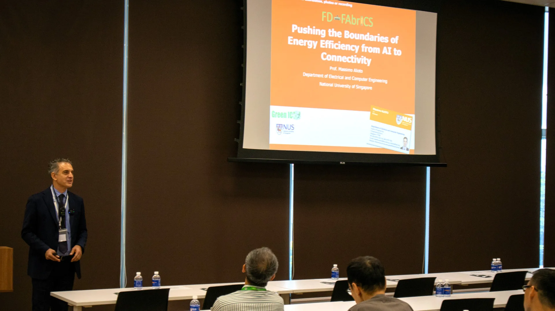
Researchers from the National University of Singapore (NUS), in collaboration with Soitec and NXP Semiconductors, have developed a new chip technology that significantly improves the energy efficiency of AI connected devices. The technology, demonstrated in fully-depleted silicon-on-insulator (FD-SOI) systems, could extend the battery life of wearables and smart objects by ten times and halve the power consumption associated with wireless communications. The breakthroughs will be promoted through the FD-SOI & IoT Industry Consortium to accelerate industry adoption. Professor Massimo Alioto, Director of the FD-fAbrICS joint lab, said the technology could move intelligence from the cloud to smart miniaturized devices.
Advancements in Chip Technology for AI Devices
Researchers from the National University of Singapore (NUS), in collaboration with industry partners Soitec and NXP Semiconductors, have developed a new class of silicon systems that could significantly enhance the energy efficiency of AI connected devices. This development could potentially revolutionize the semiconductor industry in Singapore and beyond. The innovation was demonstrated using fully-depleted silicon-on-insulator (FD-SOI) technology, which can be applied to the design and fabrication of advanced semiconductor components for AI applications.
The new chip technology could potentially extend the battery life of wearables and smart objects by a factor of 10, support intense computational workloads for use in Internet of Things applications, and halve the power consumption associated with wireless communications with the cloud. The FD-SOI & IoT Industry Consortium will promote these disruptive chip technologies to accelerate industry adoption by lowering the design barrier to entry in FD-SOI chips.
The Impact of FD-SOI Technology on AI Devices
The new suite of technologies was engineered at the FD-fAbrICS (FD-SOI Always-on Intelligent & Connected Systems) joint lab. The lab’s director, Professor Massimo Alioto, highlighted that IoT devices often operate on a very limited power budget and require extremely low average power to efficiently perform regular tasks such as physical signal monitoring. At the same time, high peak performance is demanded to process occasional signal events with computationally-intensive AI algorithms.
The applications of this technology are wide-ranging and include smart cities, smart buildings, Industry 4.0, wearables, and smart logistics. The remarkable energy improvements obtained in the FD-fAbrICS program are a game changer in the area of battery-powered AI devices, as they ultimately allow us to move intelligence from conventional cloud to smart miniaturised devices.
Accelerating Industry Adoption and Market Reach
The research conducted by the NUS FD-fAbrICS joint lab showed that their FD-SOI chip technology can be deployed at scale with enhanced design and system integration productivity for lower cost, faster market reach, and rapid industry adoption. This innovation has the potential to accelerate the time to market for key players in Singapore’s semiconductor ecosystem.
The research breakthroughs from the NUS FD-fAbrICS joint lab leverage the combined NUS expertise and capabilities from different domains, such as digital circuits, wireless communications, system architectures, and AI models. Industry leaders such as Soitec, NXP and Dolphin Design contributed to the research efforts at the joint lab, which is also supported by the Agency for Science, Technology and Research.
Future Developments in Intelligent and Connected Silicon Systems
The NUS research team is now looking into developing new classes of intelligent and connected silicon systems that could support larger AI model sizes (“large models”) for generative AI applications. The resulting decentralisation of AI computation from cloud to distributed devices will simultaneously preserve privacy, keep latency at a minimum, and avoid wireless data deluge under the simultaneous presence of a plethora of devices.
FD-SOI & IoT Industry Consortium: A Catalyst for Innovation
The FD-SOI & IoT Consortium was established to extend the impact of the NUS FD-fAbrICS joint lab on the semiconductor ecosystem in Singapore. Soitec and NXP are founding members of the Consortium. Consortium members will have access to innovative FD-SOI design IP and methodologies, which will help to accelerate their next-generation prototyping and development cycle with highly energy efficient processes, especially in the fast-growing area of AI-connected chips. The Consortium will support the near-term needs of industry for rapid technology road mapping and accelerated innovation cycle.
External Link: Click Here For More


