The pursuit of robust and controllable superconducting devices receives a significant boost from new research into semiconductor-superconductor hybrids, as Sjoerd Telkamp, Zijin Lei, and Tommaso Antonelli, alongside colleagues at Georg Jakobs’ institution, demonstrate a promising new platform. They fabricate devices using indium antimonide and niobium, creating a system with enhanced properties compared to conventional materials, including a stronger interaction between electron spin and motion, and a higher operating temperature for superconductivity. The team achieves a remarkably clean interface between the semiconductor and superconductor through a unique deposition process, resulting in a substantial induced superconducting gap. This advancement enables the creation of functional devices, such as a gate-tunable superconducting loop, and positions this material combination as a leading candidate for exploring novel states of matter and building future topological quantum devices.
Scientists present a novel semiconductor-superconductor hybrid material, combining an indium arsenide antimonide surface quantum well with a niobium top layer deposited directly onto it. This innovative material leverages the strong spin-orbit interaction of indium arsenide antimonide and the larger superconducting gap and critical magnetic field of niobium, exceeding the limitations of conventional aluminium-based systems. The in-situ deposition process creates a remarkably high-quality interface, enabling strong coupling between the semiconductor and superconductor. Experiments demonstrate an induced superconducting gap of 1. 3 meV within the indium arsenide antimonide quantum well, confirming effective transfer of superconducting properties.
InAsSb-Nb Hybrid Fabrication Details
This research involved the meticulous fabrication of devices based on an indium arsenide antimonide-niobium heterostructure, crucial for achieving high critical current densities. The fabrication process included mesa etching using both reactive-ion etching and wet chemical etching to define the active device area, followed by selective niobium etching to create Josephson junctions. An aluminium oxide/hafnium oxide dielectric layer was then deposited for insulation, and a titanium/gold top gate was fabricated, with wire bonding providing electrical connections. Additional Josephson junctions, measuring 100nm by 4μm and 75nm by 4μm, consistently exhibited high critical current densities and strong gate tunability, with a gate voltage of -2V sufficient to fully switch off both junctions within the SQUID.
Theoretical modeling described the phase escape mechanisms within the Josephson junctions, combining macroscopic quantum tunneling and thermal activation. A sigmoid interpolation smoothly transitioned between these regimes, incorporating equations for tunneling and activation rates, barrier height, and switching current. Weak antilocalization measurements characterized the spin-orbit interaction strength within the indium arsenide antimonide quantum well, revealing a large spin-orbit coupling coefficient that increases with carrier density, suggesting potential for topological superconducting devices. The effective mass of carriers within the quantum well was determined to be approximately 0.
025 electron masses. Detailed analysis of the growth process, etching procedures, dielectric deposition, and top gate fabrication provides a comprehensive understanding of the materials and fabrication techniques. These findings demonstrate the fabrication of high-performance Josephson junctions with high critical current densities, strong spin-orbit interaction, and gate tunability, supporting the claim that this heterostructure is a promising platform for realizing topological superconducting devices.
InAsSb-Nb Hybrid Achieves Strong Superconductivity
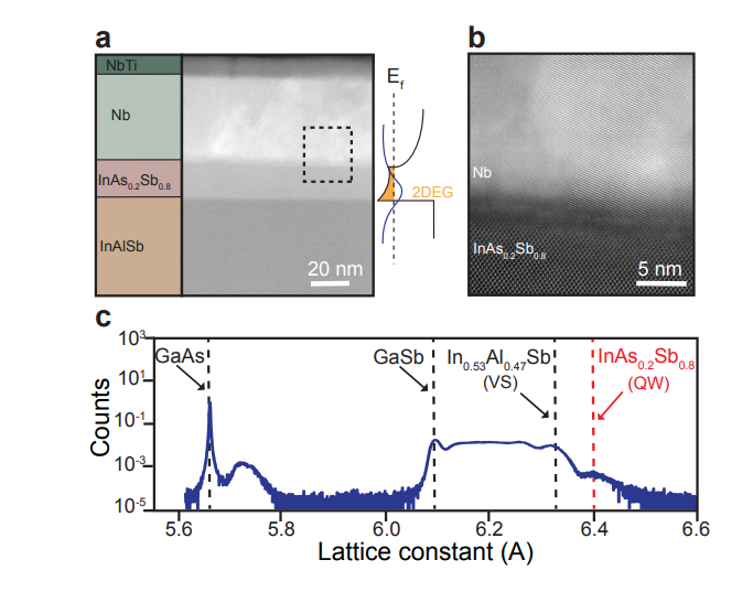
Scientists have achieved a significant breakthrough in semiconductor-superconductor hybrid materials, creating a novel platform based on an indium arsenide antimonide surface quantum well with a niobium top layer deposited directly onto it. This new material combines the strong spin-orbit interaction of indium arsenide antimonide with the larger superconducting gap and critical magnetic field of niobium, surpassing the performance limitations of conventional aluminium-based systems. The in-situ deposition process results in a remarkably high-quality interface, enabling strong coupling between the semiconductor and superconductor. Experiments reveal an induced superconducting gap of 1.
3 meV within the indium arsenide antimonide quantum well, demonstrating effective transfer of superconducting properties. High-angular dark-field scanning transmission electron microscopy confirms a crystalline interface between niobium and indium arsenide antimonide with minimal observable intermixing, suggesting the incorporation of antimony atoms limits unwanted alloy formation. Researchers fabricated a planar asymmetric Superconducting Quantum Interference Device (SQUID) exhibiting gate-tunable superimposed oscillations, originating from both the individual Josephson junction and the full SQUID loop, confirming device functionality. X-ray diffraction analysis further validates the material’s composition and crystalline structure.
The team demonstrated epitaxial growth, with the niobium layer aligning with the indium arsenide antimonide quantum well over grain domains exceeding 20nm in size. This achievement positions the material as a promising platform for exploring gate-tunable superconductivity and investigating topological superconducting devices, potentially enabling advancements in quantum computing and novel electronic applications. The combination of a large induced gap and strong spin-orbit interaction unlocks new possibilities for manipulating and controlling superconducting states within the semiconductor heterostructure.
Hybrid Material Enables Gate-Tunable SQUID Operation
This research demonstrates a novel semiconductor-superconductor hybrid material, created by combining an indium arsenide antimonide surface well with a niobium layer deposited directly onto it. The resulting structure exhibits a substantial induced superconducting gap of 1. 3 meV, significantly larger than that observed in conventional aluminium-indium arsenide systems. This achievement stems from the high-quality interface created by the in-situ deposition process, which facilitates strong coupling between the semiconductor and the superconductor. The team successfully fabricated a planar asymmetric Superconducting Quantum Interference Device (SQUID) using this hybrid material, revealing gate-tunable interference patterns originating from both individual Josephson junctions and the complete SQUID loop.
These observations confirm the potential of this platform for exploring tunable superconductivity and developing advanced quantum devices. Researchers acknowledge that variations in the observed interference patterns may arise from asymmetries between the two Josephson junctions within the SQUID, a common characteristic of these devices. This work establishes indium arsenide antimonide two-dimensional electron gases combined with large-gap superconductors as a promising platform for future research into topological quantum technologies. The team highlights the large critical current and elevated operating temperature of their Josephson junctions as key advantages for practical applications.
🗞 An InAsSb surface quantum well with in-situ deposited Nb as a platform for semiconductor-superconductor hybrid devices
🧠 ArXiv: https://arxiv.org/abs/2510.00711


