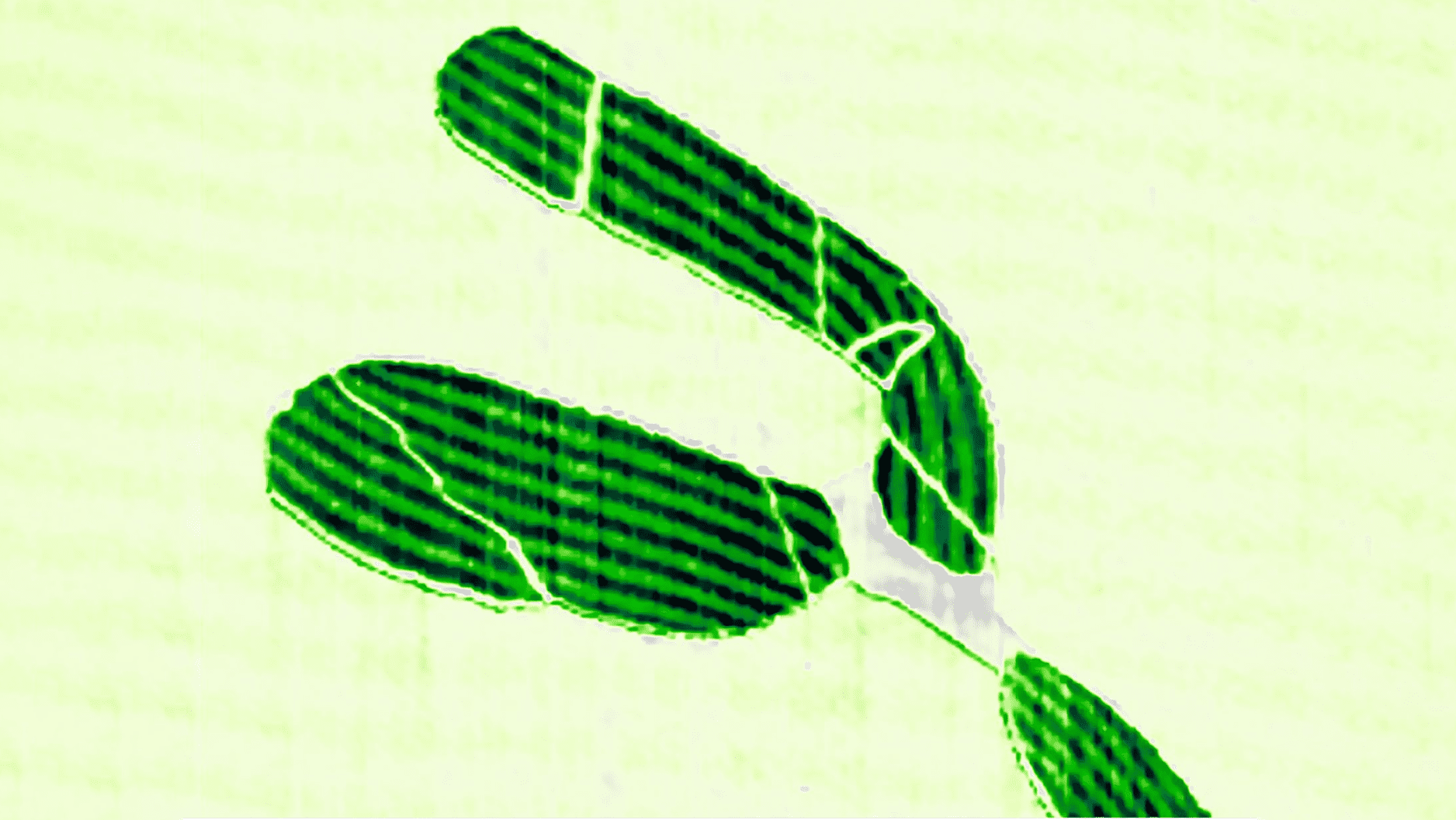
Researchers at NYU Tandon School of Engineering led by Elisa Riedo have made a groundbreaking discovery in graphene research that could revolutionize quantum applications. Graphene, a highly conductive and flexible material, has been found to self-organize into specific stacking arrangements, known as ABA and ABC stacking domains, without manual twisting or alignment.
This breakthrough, published in the Proceedings of the National Academy Of Sciences, was achieved by growing three-layer epitaxial graphene systems on silicon carbide and using advanced conductive atomic force microscopy to observe the self-assembly of these domains.
According to Riedo, controlling the size and location of these stacking patterns could be possible through pregrowth patterning of the substrate. This discovery has the potential to lead to transformative applications in quantum devices, including unconventional quantum Hall effects and superconductivity. It also brings scientists closer to realizing the full potential of graphene in next-generation electronics and quantum technologies, with funding provided by the US Army Research Office.
Introduction to Graphene and its Properties
Graphene, a single layer of carbon atoms arranged in a two-dimensional honeycomb lattice, has been extensively studied due to its exceptional properties. These properties include incredible strength, approximately 200 times stronger than steel, light weight, flexibility, and excellent electricity and heat conduction. The unique combination of these properties has made graphene an increasingly important material in various applications across fields such as electronics, energy storage, medical technology, and quantum computing. Graphene’s quantum properties, including superconductivity and other unique quantum behaviors, are known to arise when graphene atomic layers are stacked and twisted with precision to produce specific stacking domains.
The ability of graphene to exhibit these exceptional properties is highly dependent on the arrangement of its atomic layers. Historically, achieving specific stacking arrangements required exfoliating graphene and manually twisting and aligning layers with exact orientations, a process that is not only intricate but also difficult to scale for industrial applications. This limitation has hindered the widespread adoption of graphene in advanced technologies, particularly in quantum computing where precise control over the material’s properties is crucial.
Recent advancements in graphene research have focused on developing scalable methods for producing high-quality graphene with controlled stacking arrangements. One such approach involves the growth of epitaxial graphene on silicon carbide (SiC) substrates. This method allows for the production of large-area graphene with uniform properties, making it an attractive option for industrial applications. However, controlling the stacking arrangement of graphene layers during growth has remained a significant challenge.
The discovery of growth-induced self-organized ABA and ABC stacking domains in three-layer epitaxial graphene systems represents a major breakthrough in addressing this challenge. Researchers at NYU Tandon School of Engineering have observed that these specific stacking arrangements can emerge naturally during the growth process, eliminating the need for complex and non-scalable techniques traditionally used in graphene twisting fabrication.
Graphene Stacking Domains and Quantum Properties
The quantum properties of graphene, such as superconductivity and other unique quantum behaviors, are known to arise from specific stacking arrangements of its atomic layers. The most notable of these arrangements is the ABC stacking domain, which has been shown to exhibit exceptional quantum properties. However, achieving ABC stacking domains has historically required manual twisting and alignment of exfoliated graphene layers, a process that is difficult to scale.
The recent discovery of self-assembled ABA and ABC stacking domains in three-layer epitaxial graphene systems offers a promising solution to this challenge. These domains form naturally during the growth process on silicon carbide (SiC) substrates, without the need for manual twisting or alignment. The spontaneous organization of these domains represents a significant step forward in graphene stacking domains fabrication, enabling the production of high-quality graphene with controlled stacking arrangements.
The size and shape of these stacking domains are influenced by the interplay of strain and the geometry of the three-layer graphene regions. Some domains form as stripe-like structures, tens of nanometers wide and extending over microns, offering promising potential for future applications. The ability to control the size and location of these stacking patterns through pregrowth patterning of the SiC substrate could further enhance the properties of these domains.
The self-assembled ABA/ABC stacking domains have significant implications for the development of quantum devices. Their stripe-shaped configurations are well-suited for enabling unconventional quantum Hall effects, superconductivity, and charge density waves. Such breakthroughs pave the way for scalable electronic devices leveraging graphene’s quantum properties, bringing scientists closer to realizing the full potential of this remarkable material in next-generation electronics and quantum technologies.
Fabrication and Characterization of Graphene Stacking Domains
The fabrication of graphene stacking domains with controlled arrangements is a crucial step towards harnessing the unique properties of graphene. The growth of epitaxial graphene on silicon carbide (SiC) substrates offers a promising approach for producing large-area graphene with uniform properties. However, the ability to control the stacking arrangement of graphene layers during growth has remained a significant challenge.
Recent studies have demonstrated the use of advanced conductive atomic force microscopy (AFM) to characterize the self-assembled ABA and ABC stacking domains in three-layer epitaxial graphene systems. This technique enables the visualization of the domain structure and the measurement of their electrical properties, providing valuable insights into the relationship between the stacking arrangement and the quantum properties of graphene.
The use of AFM has revealed that the self-assembled domains form naturally during the growth process, without the need for manual twisting or alignment. The size and shape of these domains are influenced by the interplay of strain and the geometry of the three-layer graphene regions, resulting in stripe-like structures with promising potential for future applications.
The characterization of graphene stacking domains using AFM has significant implications for the development of quantum devices. The ability to visualize and measure the electrical properties of these domains enables researchers to optimize their structure and properties, paving the way for scalable electronic devices leveraging graphene’s quantum properties.
Applications and Future Directions
The discovery of self-assembled ABA and ABC stacking domains in three-layer epitaxial graphene systems has significant implications for the development of next-generation electronics and quantum technologies. The ability to produce high-quality graphene with controlled stacking arrangements enables the creation of scalable electronic devices that can harness the unique properties of graphene.
One of the most promising applications of graphene is in the field of quantum computing, where precise control over the material’s properties is crucial. The self-assembled ABA/ABC stacking domains offer a promising solution to this challenge, enabling the development of quantum devices with enhanced properties.
Further research is needed to fully explore the potential of graphene stacking domains and their applications. The ability to control the size and location of these domains through pregrowth patterning of the SiC substrate could further enhance their properties, enabling the creation of more complex devices with tailored properties.
The funding for this research came from the U.S. Army Research Office under Award # W911NF2020116, highlighting the significance of graphene research for future technologies. The collaboration between researchers from NYU Tandon School of Engineering and Charles University, Prague, demonstrates the global interest in graphene research and its potential to revolutionize various fields.
Conclusion
In conclusion, the discovery of self-assembled ABA and ABC stacking domains in three-layer epitaxial graphene systems represents a major breakthrough in graphene research. The ability to produce high-quality graphene with controlled stacking arrangements enables the creation of scalable electronic devices that can harness the unique properties of graphene. Further research is needed to fully explore the potential of graphene stacking domains and their applications, but the current findings offer promising solutions for the development of next-generation electronics and quantum technologies.
External Link: Click Here For More


