The quest to understand how imperfections at the atomic level influence the optical properties of materials is driving innovation in nanotechnology and optoelectronics, and recent work from Lysander Huberich, Eve Ammerman, and colleagues at Empa, alongside Gu Yu, Yining Ren from Shanghai Jiao Tong University, Sotirios Papadopoulos from ETH Z ̈urich, and Chengye Dong from Penn State, represents a significant step forward. The team directly links the atomic structure of individual defects in monolayer molybdenum disulfide (MoS ) to their unique optical signatures, achieving atomically-resolved observation of light emission. By carefully isolating MoS with a protective layer, they extended the lifetime of these defects, allowing for detailed study, and identified the distinct optical ‘fingerprints’ of common imperfections such as missing atoms, oxygen substitutions, and carbon-hydrogen complexes. This achievement establishes a crucial connection between material structure, electronic behaviour, and optical response, paving the way for the precise design and engineering of nanoscale light-emitting devices.
Defect Engineering of MoS2 Excitonic Properties
Scientists investigated the optical and electronic properties of monolayer molybdenum disulfide (MoS₂) containing defects, specifically missing atoms and carbon impurities. They employed scanning tunneling microscopy and spectroscopy to identify these defects and understand their influence on excitons, which are crucial for light emission. The team successfully imaged various defects within the MoS₂ lattice, revealing how these imperfections alter the material’s electronic structure and create changes in the band structure near the defect sites. These defects generate new excitonic states with distinct energies and properties compared to pristine MoS₂.
Researchers observed and characterized these defect-related excitons using a technique that measures emitted light, revealing that the intensity and energy of this emission can be controlled by the current flowing through the experiment. They also discovered that an electric field can shift the energy of these excitons, and that the charge state of the defects significantly impacts their optical and electronic behavior. The results demonstrate that defect emission appears at lower energies than that of pristine MoS₂, indicating direct excitation without involving the usual excitons. Detailed analysis using microscopy and spectroscopy pinpointed the location of defects and their impact on the material’s electronic structure, providing a comprehensive understanding of how these imperfections affect the material’s properties.
Van der Waals Heterostructure Fabrication and Characterization
Scientists engineered a heterostructure by layering monolayer molybdenum disulfide (MoS₂) on bilayer hexagonal boron nitride (hBN), supported by graphene. This structure was designed to investigate nanoscale optical properties, and was created using a precise transfer method followed by rigorous cleaning. Researchers distinguished between the materials using spectroscopy, observing the expected band gaps for each material, and confirmed the layer-dependent characteristics of hBN. Microscopy further identified the materials and revealed moiré superlattices in hBN due to lattice mismatch with graphene, and characteristic point defects in MoS₂.
To enhance observation, the team intentionally introduced sulfur vacancies and carbon-hydrogen complexes into the MoS₂, achieving a low initial defect density. Placing bilayer hBN between MoS₂ and graphene resulted in an increased band gap and reduced screening of electronic interactions. Spectroscopy and topography measurements confirmed that sulfur vacancies remained negatively charged, aligning with the Fermi level of the underlying graphene substrate, indicating effective electronic decoupling. The study pioneered electrically stimulated exciton emission. Supporting MoS₂ with bilayer hBN enhanced the brightness of this emission sevenfold compared to monolayer hBN, accompanied by a slight increase in emission energy consistent with the increased electronic band gap. High-resolution spectra revealed a sharp emission line, tentatively assigned to MoS₂ excitons and trions.
Atomic Structure Dictates Monolayer Optical Properties
This work establishes a direct link between atomic structure and optical properties in two-dimensional materials, specifically monolayer MoS₂, paving the way for precise engineering of quantum emitters. Scientists achieved electronic decoupling of MoS₂ from the substrate using bilayer hexagonal boron nitride (hBN), resulting in an increased band gap and extended charge state lifetime of defects. This decoupling facilitated electrically stimulated photon emission from both pristine MoS₂ excitons and trions, demonstrating enhanced optical performance. Spatially resolved spectral mapping revealed nanoscale sensitivity to local potential fluctuations, highlighting the impact of the surrounding environment on exciton behavior.
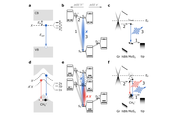
Crucially, the team identified the unique spectral fingerprints of common point defects in MoS₂, including sulfur vacancies, oxygen substitutions, and negatively charged carbon-hydrogen complexes. While sulfur vacancies and oxygen substitutions suppress emission from pristine excitons, the negatively charged carbon-hydrogen complexes generate defect-bound exciton complexes at lower energies. Measurements confirm that these defect-bound excitons exhibit a strong dependence on injection bias and current, revealing a charge-mediated excitation mechanism. Sub-nanometer-resolved luminescence maps demonstrate large spectral shifts near charged defects, concurrent with the local band bending expected for band-to-defect optical transitions. The strong correlation between probe position and spectral shift around the charged impurity is consistent with a band-to-defect transition. These results establish an atomically precise understanding of the relationship between structure, electronic states, and optical response, enabling the deterministic engineering of emitters in 2D materials.
Atomic Defects Control Monolayer Exciton Emission
This work demonstrates atomically-resolved exciton emission from monolayer molybdenum disulfide and identifies the optical signatures of individual atomic defects. By decoupling the material from its substrate with ultrathin hexagonal boron nitride layers, researchers extended the lifetime of defect charge states and enabled detailed observation of exciton and trion behavior. The study reveals that oxygen substitutions and sulfur vacancies suppress emission from pristine molybdenum disulfide, but do not generate additional defect-related emission. In contrast, negatively charged carbon-hydrogen complexes create distinct defect-bound exciton emission at lower energies than those of pristine molybdenum disulfide.
Researchers conclusively linked this emission to its atomic origin and mapped its spatial extent, demonstrating a correlation between local electronic structure and nanoscale optical response. The findings establish that this defect emission arises from an exciton bound to an ionized acceptor-like impurity resulting from a band-to-defect transition. This achievement provides fundamental insight into these interactions and establishes a pathway toward the deterministic engineering of quantum emitters in two-dimensional materials, offering potential for advanced optoelectronic devices.
🗞 Atomically-resolved exciton emission from single defects in MoS
🧠 ArXiv: https://arxiv.org/abs/2510.15676


