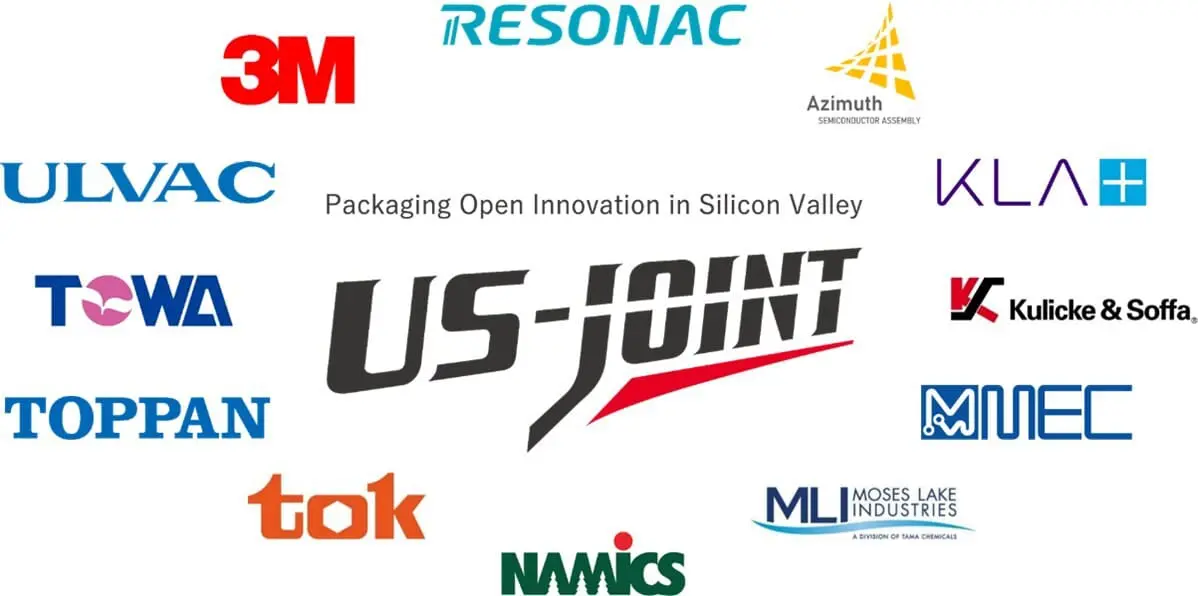
The quest for enhanced semiconductor technology has prompted 3M to join forces with the US-JOINT Consortium, a collaborative endeavor comprising 12 prominent semiconductor suppliers, to propel advancements in next-generation semiconductor packaging and back-end processing technologies.
As the demands of artificial intelligence and high-performance computing continue to escalate, the need for comprehensive solutions to intricate challenges has become increasingly pressing, prompting industry leaders to converge and leverage their collective expertise. With its rich legacy of materials science innovation spanning over 50 technology platforms, 3M is poised to make a significant contribution to the consortium, which is anchored by a state-of-the-art facility in Silicon Valley and led by Japan-based Resonac, a global powerhouse in the semiconductor and electronics industry.
This strategic partnership underscores 3M’s commitment to delivering integrated solutions for the semiconductor industry while highlighting the importance of collaborative innovation in driving technological progress and addressing the challenges ahead.
Introduction to Semiconductor Technology Advancements
The semiconductor industry is witnessing significant technological advancements, driven by the increasing demands of artificial intelligence (AI) and high-performance computing applications. Companies are forming strategic partnerships to address these challenges to accelerate research and development in next-generation semiconductor technologies. One such partnership is the US-JOINT Consortium, a collaborative effort between 12 semiconductor suppliers, including 3M, which has recently joined the consortium. The US-JOINT Consortium aims to drive innovation in advanced packaging and back-end processing technologies, focusing on developing comprehensive solutions for the industry’s toughest challenges.
The consortium’s efforts are centered around a new cutting-edge research and development facility in Silicon Valley, which is expected to be unveiled later this year. This facility will serve as a hub for collaboration and innovation, bringing together experts from various companies to work on advancing semiconductor technologies. By pooling their resources and expertise, the member companies of the US-JOINT Consortium aim to accelerate the development of next-generation semiconductor technologies, including advanced packaging and back-end processing techniques. These advancements are crucial for meeting the increasing demands of AI and high-performance computing applications, which require faster, more efficient, and more reliable semiconductor devices.
The US-JOINT Consortium’s focus on advanced packaging technologies is particularly significant, as these technologies play a critical role in enabling the development of smaller, faster, and more powerful semiconductor devices. Advanced packaging techniques, such as 3D stacking and fan-out wafer-level packaging, allow for the integration of multiple dies and components into a single package, reducing size and increasing performance. By developing new materials and processes for advanced packaging, the US-JOINT Consortium aims to enable the creation of more complex and powerful semiconductor devices, which will be essential for driving innovation in fields such as AI, autonomous vehicles, and the Internet of Things (IoT).
The Role of 3M in the Semiconductor Industry
3M has a long history of involvement in the semiconductor industry, dating back over 25 years. During this time, the company has established itself as a supplier of materials and processing aids for various semiconductor applications, including polishing, advanced packaging, and chip transport. By joining the US-JOINT Consortium, 3M is reinforcing its commitment to the semiconductor industry and expanding its role as an integrated total solutions provider. The company’s expertise in materials science, which spans over 50 technology platforms, will be a valuable asset to the consortium, enabling the development of new materials and processes for advanced packaging and back-end processing applications.
3M’s involvement in the US-JOINT Consortium is also significant because it highlights the importance of collaboration and partnership in driving innovation in the semiconductor industry. By working together with other companies, 3M can leverage its expertise and resources to address the industry’s toughest challenges and develop new technologies that will enable the creation of more powerful and efficient semiconductor devices. This collaborative approach is essential for driving progress in the semiconductor industry, where the complexity and cost of developing new technologies are increasingly prohibitive for individual companies.
The partnership between 3M and the US-JOINT Consortium also reflects the growing trend towards collaboration and cooperation in the semiconductor industry. As the demands of AI and high-performance computing applications continue to drive innovation, companies are recognizing the need to work together to develop new technologies and address common challenges. This shift towards collaboration is likely to have a profound impact on the semiconductor industry, enabling the development of more complex and powerful devices that will drive innovation in a wide range of fields.
Advanced Packaging Technologies
Advanced packaging technologies play a critical role in enabling the development of smaller, faster, and more powerful semiconductor devices. These technologies involve the integration of multiple dies and components into a single package, reducing size and increasing performance. The US-JOINT Consortium’s focus on advanced packaging is significant, as it reflects the growing importance of these technologies in driving innovation in the semiconductor industry. By developing new materials and processes for advanced packaging, the consortium aims to enable the creation of more complex and powerful semiconductor devices that will be essential for driving progress in fields such as AI, autonomous vehicles, and the IoT.
One of the key challenges in advanced packaging is the development of new materials and processes that can enable the integration of multiple dies and components into a single package. This requires the development of new dielectrics, metals, and other materials that can withstand the stresses and strains of the packaging process. The US-JOINT Consortium’s research and development efforts are focused on addressing these challenges, with a particular emphasis on developing new materials and processes for 3D stacking and fan-out wafer-level packaging. These technologies have the potential to enable the creation of highly complex and powerful semiconductor devices, with applications in a wide range of fields.
The development of advanced packaging technologies is also driving innovation in other areas of the semiconductor industry, such as chip design and manufacturing. As packages become smaller and more complex, the need for more sophisticated chip designs and manufacturing techniques becomes increasingly important. This is driving the development of new design tools and manufacturing processes, such as 3D stacked integrated circuits and hybrid bonding. These technologies have the potential to enable the creation of highly complex and powerful semiconductor devices, with applications in a wide range of fields.
The Impact of Collaboration on Innovation
The partnership between 3M and the US-JOINT Consortium highlights the growing importance of collaboration and cooperation in driving innovation in the semiconductor industry. By working together, companies can leverage their expertise and resources to address common challenges and develop new technologies that will enable the creation of more powerful and efficient semiconductor devices. This collaborative approach is essential for driving progress in the semiconductor industry, where the complexity and cost of developing new technologies are increasingly prohibitive for individual companies.
The impact of collaboration on innovation in the semiconductor industry cannot be overstated. By working together, companies can share knowledge, expertise, and resources, reducing the risk and cost of developing new technologies. This enables them to focus on high-risk, high-reward research and development projects that might not be feasible for individual companies to pursue alone. The results of these collaborative efforts are likely to have a profound impact on the semiconductor industry, enabling the development of more complex and powerful devices that will drive innovation in a wide range of fields.
The US-JOINT Consortium’s focus on collaboration and cooperation also reflects the growing recognition of the importance of ecosystem-based innovation in the semiconductor industry. This approach involves bringing together companies from across the supply chain to work together on developing new technologies and addressing common challenges. By working together, companies can create a more vibrant and dynamic ecosystem that is better equipped to drive innovation and address the complex challenges facing the industry. This collaborative approach is likely to have a profound impact on the semiconductor industry, enabling the development of more powerful and efficient devices that will drive progress in a wide range of fields.
External Link: Click Here For More


