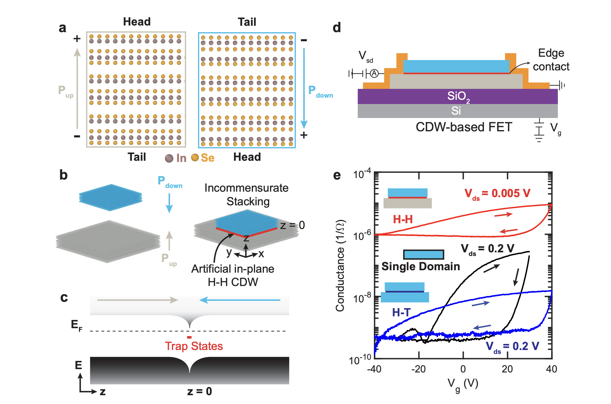
Charged domain walls, boundaries between differing regions within a material, represent a promising frontier for next-generation electronics, but realising their potential has been hampered by significant technical hurdles. Shahriar Muhammad Nahid, Haiyue Dong, and Gillian Nolan, alongside colleagues at the University of Illinois Urbana-Champaign, the University of California, Irvine, and the University of Chicago, now demonstrate a breakthrough in this field by creating functional field-effect transistors based on these domain walls within a van der Waals ferroelectric material, α-InSe. The team overcomes previous limitations by engineering artificial domain walls and establishing electrical contact, resulting in devices that exhibit dramatically improved performance compared to single-layer materials. This innovation resolves longstanding challenges with high resistance in charged domain walls and paves the way for the development of faster, more efficient electronic components, potentially enabling gigahertz-speed memory and novel computing technologies.
Controlling Ferroelectric Domain Walls for Electronics
The pursuit of faster, more energy-efficient electronics has led researchers to explore novel materials and device concepts, and ferroelectric domain walls are emerging as particularly promising candidates. These walls, which separate regions of differing polarization within a ferroelectric material, possess unique electrical properties that could revolutionize nonvolatile memory, logic circuits, and even artificial intelligence. However, realizing this potential has been hampered by challenges in creating and accessing these walls within conventional materials. Traditionally, domain walls in ferroelectrics have been oriented vertically or buried, making electrical contact and control difficult.
Furthermore, their electrical resistance has been exceedingly high, limiting speed and efficiency. Researchers have sought ways to overcome these obstacles and create electrically accessible, low-resistance domain walls suitable for integration into advanced electronic circuits. Recent work presents a breakthrough in this field, demonstrating a method for creating artificial domain walls with significantly enhanced conductivity. This approach involves stacking layers of a ferroelectric material in a specific configuration, allowing for the creation of electrically accessible interfaces and overcoming many of the limitations of conventional domain wall devices.
Charged Domain Walls Enable High Conductivity
Results resolve longstanding challenges with high charged domain wall (CDW) resistance and their device integration, opening opportunities for gigahertz memory and neuromorphic computing. Ferroelectric domain walls are emerging as novel functional interfaces, where their reduced dimensionality and different symmetry generate distinct properties, such as polarity, enhanced electromechanical coupling, or conducting states. Of particular interest are charged domain walls, where adjacent domains with opposite polarization meet to create interfacial bound charges which require screening by free carriers, resulting in orders of magnitude higher conductivity compared to bulk domains. While enhanced CDW conductivity was predicted decades ago, experimental confirmation came in 2009 in BiFeO3.
Since then, the field has expanded, leading to the realization of conducting CDWs in various ferroelectrics, including BaTiO3, PZT, and LiNbO3. In most cases, these domain walls are oriented along the out-of-plane direction and exhibit lower resistance compared to surrounding bulk domains. Other systems show mobile CDWs under electric field, but these have been difficult to electrically access for transport measurements. These results have led to potential applications in nonvolatile memory, logic, and artificial synapses, demanding new strategies to create in-plane, electrically accessible, and gate-tunable CDWs that may be integrated into devices, as well as a more complete understanding of the mechanisms and limits of interfacial conduction.
Artificial Ferroelectric Charge Density Wave Conductivity
Researchers demonstrate a robust method for generating highly conducting ferroelectric charge density waves (CDWs) and integrating them into functional devices. This method of creating artificial CDWs should be universally applicable to any van der Waals ferroelectric with out-of-plane polarization. These artificial CDWs show two modes of conduction: high temperature trap assisted transport and low temperature variable range hopping (VRH) transport. Despite having the lowest polarization, these CDWs show the lowest resistance compared to other ferroelectric CDWs reported in the literature. Further improvement is possible by controlling twist angle, interfacial roughness, and defects.
Fabrication of these structures involves stacking two α-In2Se3 flakes on top of one another, mechanically exfoliated and transferred using standard techniques. Piezoresponse force microscopy (PFM) is used to confirm the polarization direction of each flake to identify the desired configuration. Fabrication of field-effect transistors (FETs) based on α-In2Se3 single domains, heterostructures, and CDWs involves standard electron-beam lithography, metal deposition, and lift-off processes. Electronic transport and magneto-transport measurements are performed using a Physical Property Measurement System (PPMS).
Output and transfer characteristics of the FETs are measured using a Keithley 4200A-SCS Parameter Analyzer. Four-terminal magneto-transport measurements are completed using a lock-in amplifier. Samples are prepared for cross-sectioning by applying a protective coating of amorphous carbon via thermal evaporation. STEM imaging and electron energy loss spectroscopy (EELS) of cross-sectional samples are completed using aberration-corrected STEM. This work was supported by NSF-MRSEC under Award Number DMR- and carried out in part at the Materials Research Laboratory Central Facilities at the University of Illinois.
S.M.N. fabricated the heterostructures and performed AFM and PFM characterizations. S.M.N. and H.D. fabricated and characterized the electrical transport and magneto-transport of the devices.
G.N. performed the STEM imaging. All authors read and contributed to the manuscript. The data can be accessed for review at the Illinois Data Bank, DOI:. The authors declare no competing financial interest.
🗞 Field-effect transistors based on charged domain walls in van der Waals ferroelectric α-In Se
🧠 DOI: https://doi.org/10.48550/arXiv.2507.09838


