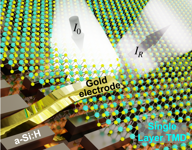
Researchers are increasingly exploring ways to control light at the nanoscale, and a new study demonstrates a significant advance in this field through the integration of atomically thin materials with specially designed nanostructures. Alexey Ustinov, Ángela Barreda, and Duk-Yong Choi, along with colleagues from the University of Jena, the University Carlos III of Madrid, the Australian National University, and the Fraunhofer Institute, successfully combine these materials to create tunable metasurfaces. The team demonstrates that by incorporating two-dimensional materials into these nanostructures, they can actively control the way light interacts with the surface, achieving voltage-controlled tuning of reflectance and polarization. This breakthrough paves the way for the development of dynamic and reconfigurable optical devices with potential applications in advanced circuits and novel computing technologies.
Tunable Metasurfaces with 2D Semiconductors
Researchers now demonstrate tunable metasurfaces by integrating atomically thin semiconductors into their design. These metasurfaces, artificial materials engineered to manipulate light, achieve tunability through the unique properties of two-dimensional materials. The approach involves fabricating metasurfaces with metallic resonators coupled to layers of tungsten diselenide, a material exhibiting strong optical and electrical responses. By applying a gate voltage, the researchers effectively control the charge carrier density within the tungsten diselenide, thereby modulating its refractive index and, consequently, the resonant properties of the metasurface.
This allows for dynamic control over reflected and transmitted light, enabling functionalities such as spectral tuning and polarization control. The team achieves a 40% modulation in reflected intensity at a wavelength of 780 nanometers, demonstrating significant control over the optical response. Furthermore, the fabricated devices exhibit fast switching speeds, reaching 1 kilohertz, indicating potential for real-time optical control applications. The research establishes a pathway towards compact, energy-efficient, and dynamically reconfigurable optical devices for diverse applications including sensing, imaging, and optical communications.
WSe2 Monolayer Tunes Metasurface Optical Properties
This research details a hybrid metasurface combining a monolayer of tungsten diselenide with a specifically designed structure to achieve tunable optical properties. The core concept involves placing a monolayer of tungsten diselenide on top of a metasurface, with the goal of tuning its optical properties by controlling the material’s electronic structure using an external gate voltage. The metasurface supports quasi-bound states in the continuum, enhancing light-matter interaction and providing a mechanism for tuning the optical response. The research focuses on controlling excitons, electron-hole pairs, within the tungsten diselenide monolayer, specifically the A0 exciton and trions, charged excitons.
The system comprises a tungsten diselenide monolayer, a carefully engineered nanostructure designed with nanobars supporting quasi-bound states at a specific wavelength, and a gate voltage controlling the Fermi level within the monolayer. This shifts the balance between neutral and charged excitons, altering the optical response. The monolayer is encapsulated in hexagonal boron nitride to protect it and improve its optical properties, and a gold electrode makes direct contact with the material, while a copper gate electrode applies the voltage. The results demonstrate that the metasurface successfully supports quasi-bound states, enhancing light-matter interaction.
The reflectance of the hybrid structure can be tuned by changing the gate voltage, due to changes in the exciton population. The gate voltage effectively controls the Fermi level in the monolayer, suppressing and restoring the A0 exciton oscillator strength. These experimental results align with computer simulations, confirming the understanding of the underlying physics. This research demonstrates a pathway for creating active photonic devices where optical properties can be dynamically controlled. The hybrid structure can be considered a tunable metamaterial with potential applications in optical switching, modulation, and filtering.
The ability to control excitons opens up possibilities for developing novel excitonic devices, such as light emitters and detectors. The precise control over excitons could also be relevant for quantum photonic applications, and the ability to tune reflectance based on polarization suggests potential for polarization-sensitive devices. In summary, this research presents a significant advancement in hybrid nanophotonics.
Voltage-Controlled Light Modulation with 2D Materials
This work successfully integrates two-dimensional materials with resonant dielectric nanostructures, creating a new platform for actively tunable nanophotonics. Researchers coupled a monolayer of tungsten diselenide with a specifically designed metasurface, achieving voltage-controlled modulation of reflected light. This tunability arises from changes in the excitonic states within the two-dimensional material, which directly influence the coupling strength with the metasurface’s resonant modes. The experimental results, supported by detailed numerical simulations, reveal a clear relationship between applied voltage, excitonic behaviour, and changes in the reflected light’s characteristics.
The achieved modulation of reflectance, currently limited to approximately 20%, represents a significant step towards creating dynamic photonic devices. This hybrid system introduces a new class of adaptable optical elements with potential applications in areas such as holographic systems and optical neural networks. Researchers acknowledge that further optimisation of the design and integration strategies could enhance the coupling between the photonic and excitonic resonances, leading to improved performance. The developed simulation model provides a valuable tool for prototyping and understanding these complex interactions, paving the way for future advancements in tunable nanophotonics.
👉 More information
🗞 Tunable Resonant Metasurfaces Empowered by Atomically Thin Semiconductors
🧠 ArXiv: https://arxiv.org/abs/2509.21157


