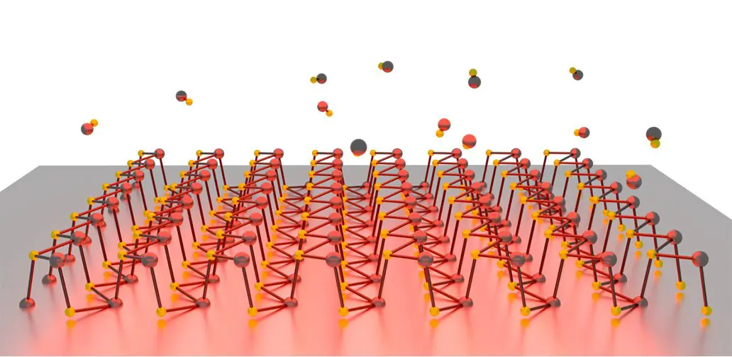
Researchers at Tohoku University, the National Institutes for Quantum Science and Technology (QST), and Cambridge University have achieved a breakthrough in the synthesis of tin sulfide (SnS), a semiconductor material with potential applications in next-generation electronics. The team has developed a streamlined and cost-effective method for growing SnS in single-atom-thick layers – known as a monolayer – overcoming a key obstacle in the material’s wider adoption. This advance promises to facilitate research into ‘spin-valleytronics’, an emerging field aiming to enhance computational efficiency by exploiting the quantum properties of electrons. It could pave the way for faster, more compact devices. The findings, published in Nano Letters, detail a process of precisely controlling the vapour deposition of tin and sulphur onto silicon wafers to produce high-quality SnS crystals selectively.
The controlled synthesis of monolayer tin sulfide (SnS) represents a significant advance in two-dimensional materials science, potentially enabling innovations in wave-parallel computing and spin-valleytronic devices. Researchers at Tohoku University, the National Institutes for Quantum Science and Technology (QST), and Cambridge University have demonstrated a novel method for reliably producing large-area, single-layer SnS films directly on silicon wafers. Prior attempts to create pure SnS have been hindered by the tendency of tin and sulfur precursors to form alternative compounds, notably tin disulfide (SnS2), which necessitates complex and often inefficient fabrication processes.
The team’s approach, detailed in Nano Letters, leverages a carefully controlled vapour-phase reaction. By precisely regulating the relative abundance of sulfur and tin during sublimation – the direct transition from solid to gaseous state – the researchers were able to direct the formation of SnS. This control is predicated on a computer-modelled phase diagram, which predicted that a lower sulfur partial pressure would favour SnS formation, while higher concentrations would promote SnS2. Experimental validation involved systematically varying the distance between the sulfur source and the tin substrate, effectively modulating the sulfur flux during the growth process.
Crucially, the process was monitored *in situ* using
Crucially, the process was monitored in situ using operando scanning electron microscopy. This technique allowed researchers to observe the sublimation of excess material, leaving behind a monolayer film of highly pure SnS. The ability to witness this process in real-time provided crucial insights into the growth mechanism and confirmed the effectiveness of their compositional control strategy. The resulting films exhibit a uniformity and purity previously unattainable, paving the way for more reliable and reproducible device fabrication. This level of control is particularly critical for exploiting the unique electronic and optical properties of SnS in advanced applications, where even minor variations in composition can significantly impact performance.
The key lies in SnS’s unique electronic and optical characteristics. Unlike conventional semiconductors, SnS demonstrates a complex interplay between charge, spin, and valley degrees of freedom. ‘Valleytronics’, a nascent field of research, seeks to exploit the ‘valley’ – a quantum mechanical property relating to the energy minima within a material’s electronic band structure – as a means of encoding and processing information. By manipulating the valley state of electrons within SnS, it may be possible to create devices with significantly enhanced efficiency and functionality. This is further compounded by the material’s inherent spin properties, aligning it with the principles of ‘spintronics’ – a technology that leverages electron spin, rather than charge, to carry information. The convergence of ferroelectric, spintronic, and valleytronic principles within a single material represents a potentially transformative step towards novel computing architectures.
Current semiconductor technology, predicated on the continued miniaturisation
Current semiconductor technology, predicated on the continued miniaturisation of silicon-based transistors, is approaching fundamental physical limits. The pursuit of alternative materials capable of surpassing these constraints is therefore critical. The ability to consistently produce monolayer SnS opens avenues for exploring wave-parallel computing. This paradigm, distinct from traditional von Neumann architectures, relies on manipulating waves – in this case, electronic excitations within the material – to perform computations. The unique band structure of SnS, coupled with its valleytronic properties, could facilitate the creation of devices capable of processing information in a massively parallel fashion, potentially leading to substantial gains in computational speed and energy efficiency. While significant engineering challenges remain in translating these materials properties into functional devices, the demonstrated control over SnS synthesis represents a crucial step towards realising the potential of this material in advanced computing applications. The ability to reliably produce large-area, monolayer SnS with defined stoichiometry is therefore a crucial step towards realising the potential of this material in next-generation electronic devices.
More information
External Link: Click Here For More


