Strain offers a powerful means to manipulate the electronic characteristics of semiconductors, and Samuel D. Escribano, Alfredo Levy Yeyati, and Elsa Prada, from the Weizmann Institute of Science, Universidad Autónoma de Madrid, and CSIC respectively, have developed a new model to accurately capture these effects in crucial III-V semiconductors. Current simulation methods often struggle to balance accuracy with computational efficiency, particularly when considering the impact of strain, and this work addresses that challenge by deriving a compact Hamiltonian that describes the conduction band of these materials. The resulting model reproduces the behaviour predicted by more complex calculations, yet remains practical for simulating the properties of nanoscale devices, offering a versatile tool for designing advanced technologies. This achievement promises to accelerate progress in fields such as spintronics, straintronics, optoelectronics, and topological materials by enabling reliable predictions of semiconductor behaviour under strain.
However, for III-V compounds, key materials for quantum applications, such approaches remain comparatively underdeveloped. This work derives a compact, effective Hamiltonian that describes the conduction band of zincblende III-V semiconductors incorporating strain effects, starting from the eight-band k⋅p model with Bir, Pikus correction.
Strain Effects on Nanowire Band Structure
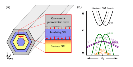
Scientists have undertaken a detailed computational study of semiconductor nanowires, focusing on understanding how strain influences their electronic behavior. The research employs a sophisticated eight-band k⋅p perturbation method to accurately describe the electronic band structure of materials like indium arsenide, indium antimonide, gallium arsenide, and gallium antimonide. This advanced approach allows for a more precise understanding of material properties than simpler effective mass approximations. The team defined a comprehensive set of material parameters essential for the eight-band k⋅p model, including band gap, spin-orbit split-off energy, and parameters describing the heavy-hole band. These parameters were used in simulations of nanowire structures with varying layer thicknesses, core radii, and surface charge densities, conducted at extremely low temperatures to isolate the effects of strain and geometry. The team meticulously modeled core-double shell nanowire architectures, where an insulating semiconductor confines electron transport to an active shell experiencing strain due to lattice mismatch.
Strain Effects on Zincblende Semiconductor Bands
Scientists have developed a compact analytical model to accurately describe the behavior of electrons in zincblende III-V semiconductors under mechanical strain, a crucial factor in modern nanoscale devices. The research delivers comprehensive analytical expressions that capture the impact of strain on the conduction band of these materials, providing a versatile tool for device design and prediction of material properties. The team derived an effective Hamiltonian that incorporates strain effects through renormalized parameters, accurately reproducing results obtained with more complex multiband calculations for small to moderate strain levels. Researchers demonstrated that any deformation, excluding rotation, can be expressed as a combination of hydrostatic, biaxial deviatoric, and pure shear deformation, providing a complete framework for understanding strain effects.
Analysis of bulk semiconductors reveals how strain modifies key electronic properties, enabling precise control over material behavior. Furthermore, the team applied this model to one-dimensional nanowires and two-dimensional heterostructures, demonstrating how strain can be harnessed to enhance desirable properties or compromise device performance. Specifically, they explored a core-double shell nanowire architecture, where an insulating semiconductor confines electron transport to an active shell experiencing strain due to lattice mismatch, allowing for tunable spin-orbit coupling and effective g-factor, potentially creating functional straintronic nanodevices. The work provides a framework for detecting strain within these nanostructures and optimizing their properties through targeted stress engineering.
Strain’s Impact on Semiconductor Electronic Properties
This work presents a new analytical framework for understanding how mechanical strain impacts the electronic properties of zincblende III-V semiconductor compounds, materials crucial for advanced technologies. Researchers developed a compact model, derived from a detailed eight-band k⋅p approach, that accurately describes the conduction band while incorporating the effects of strain. This model provides analytical equations for key parameters, effective mass, chemical potential, spin-orbit coupling, and g-factor, allowing for efficient calculation of strain-induced changes in these properties. Validation against full numerical calculations confirms the model’s accuracy for both small and moderate strain levels, and its application to core-shell nanowires and two-dimensional heterostructures demonstrates its versatility.
The team observed significant strain anisotropy, particularly in spin-orbit interaction and the g-tensor, revealing how strain can be used to tune these properties. This capability has implications for designing spin-field-effect transistors and next-generation topological nanodevices, where strong spin-orbit coupling is essential for robust performance. A comprehensive set of parameters for a broader range of III-V compounds is also provided. The researchers suggest that combining intrinsic strain from lattice mismatch with externally applied stress via piezoelectric materials offers a promising route toward engineering spin-orbit coupling and g-factors on demand, establishing strain as a key design parameter for future quantum devices.
👉 More information
🗞 Effective conduction-band model for zincblende III-V semiconductors in the presence of strain: tuning the properties of bulk crystals and nanostructures
🧠 ArXiv: https://arxiv.org/abs/2509.13246


