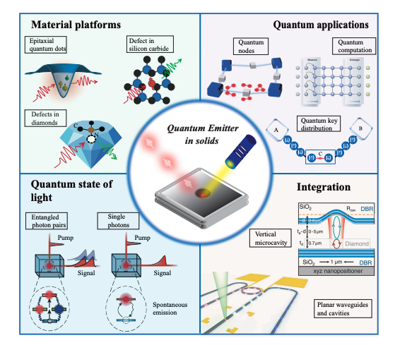
Quantum emitters – nanoscale light sources – represent a key component for scalable quantum technologies. Recent research focuses on three material platforms – quantum dots, diamond defect centres and silicon carbide defect centres – demonstrating advancements in quantum communication and sensing capabilities, with ongoing work addressing performance optimisation and future challenges.
The demand for reliable, scalable sources of single photons and entangled photon pairs is intensifying as quantum technologies transition from theoretical possibility to practical application. These quantum states of light underpin advances in secure communication, precision sensing, and quantum computation, requiring emitters integrated directly into solid materials for robust and reproducible performance. Researchers at the University of Electronic Science and Technology of China, led by Shicheng Yu, Xiaojie Zhang, Xia Lei, and Liang Zhai, address this need in a comprehensive review titled ‘A Concise Primer on Solid-State Quantum Emitters’. Their work surveys the fundamental principles governing these devices, focusing on three prominent material systems – quantum dots, diamond defect centres (specifically nitrogen-vacancy centres), and silicon carbide defect centres – and provides a comparative analysis of their strengths and limitations for future quantum technologies.
Quantum Emitters: Solid-State Sources for Emerging Technologies
Quantum emitters function as deterministic sources of quantum states of light, such as single and entangled photons, and serve as interfaces between light and matter. Their solid-state nature facilitates adoption of established nanofabrication techniques, enabling precise environmental control crucial for scalable quantum technologies. This review details the fundamentals of quantum emitters, key performance metrics, and recent developments across three prominent material platforms – quantum dots, defect centres in diamond, and defect centres in silicon carbide – assessing their progress in quantum communication, computation, and sensing.
Researchers continually refine the efficiency and coherence of these emitters to optimise performance. Key metrics for evaluation include emission wavelength, brightness (photon count rate), indistinguishability (essential for multi-photon interference), and coherence time (the duration quantum information is preserved).
Quantum dots, semiconductor nanocrystals exhibiting quantum mechanical properties, offer strong light emission. However, their coherence is often limited by interactions with the surrounding environment. Mitigation strategies include surface passivation (reducing surface defects), core-shell structures (encapsulating the dot to minimise surface effects), and embedding within protective matrices. These approaches aim to reduce decoherence – the loss of quantum information – and enhance quantum properties.
Diamond defect centres, notably the nitrogen-vacancy (NV) centre, exhibit long coherence times and operate at room temperature. This makes them attractive for quantum sensing and information processing. The NV centre’s unique electronic structure and symmetry properties provide protection from environmental noise, preserving quantum information for extended periods. Current research focuses on controlling and manipulating the NV centre’s spin state to implement quantum algorithms and develop novel sensors. Integrating NV centres into photonic structures promises to enhance light-matter interaction and facilitate efficient quantum interfaces.
Silicon carbide (SiC) defect centres, particularly those involving silicon and carbon vacancies, are gaining prominence. They offer a compelling combination of compatibility with existing semiconductor infrastructure and intriguing quantum properties. SiC’s wide bandgap and high thermal conductivity make it suitable for high-power and high-temperature applications. Its defect centres exhibit promising coherence properties and potential for integration into photonic circuits. Researchers are actively investigating various SiC defect centres, exploring their optical and spin properties and developing techniques for controlling their quantum states. As with diamond NV centres, integrating SiC defect centres into photonic structures aims to enhance light-matter interaction and create efficient quantum interfaces.
Each platform presents distinct advantages and disadvantages. Quantum dots offer relatively simple fabrication but suffer from limited coherence. Diamond NV centres boast long coherence times but are expensive and challenging to integrate into complex circuits. SiC defect centres offer a potential compromise, leveraging existing semiconductor manufacturing processes while exhibiting promising quantum properties.
Addressing several key challenges is crucial for realising practical quantum systems. These include extending coherence times, enhancing light-matter interaction, and developing scalable fabrication techniques. Further research must focus on a deep understanding of the underlying physics governing quantum emitters and the development of innovative materials and device architectures. A collaborative approach between researchers, engineers, and industry partners is essential to foster innovation and unlock the full potential of quantum emitters in building robust and reliable quantum technologies.
👉 More information
🗞 A Concise Primer on Solid-State Quantum Emitters
🧠 DOI: https://doi.org/10.48550/arXiv.2506.06684


