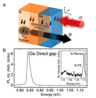
Researchers demonstrate efficient spin polarization in silicon via an all-analog spin pumping technique, utilising a germanium-on-silicon heterostructure. This achieves a polarization degree of up to 9%, facilitated by effective spin injection and shortened carrier lifetimes due to defects. This advances the potential for silicon spintronics, overcoming limitations inherent in its band structure.
The manipulation of electron spin, a quantum property akin to angular momentum, presents a significant challenge in the development of advanced technologies, particularly within silicon-based spintronics. Silicon, despite its dominance in conventional electronics, exhibits limited optical activity, hindering efficient spin control via traditional methods. Researchers are now demonstrating a novel approach to overcome this limitation, utilising a process termed ‘spin pumping’ to transfer spin polarisation from a germanium absorber to a silicon layer within a heterostructure. This technique achieves a remarkable 9% polarisation degree in emitted silicon light, a substantial improvement over previous attempts. The work, detailed in a forthcoming publication, is the result of a collaborative effort led by Stefano Achilli, Damiano Marian, Mario Lodari, Emiliano Bonera, Giordano Scappucci, Jacopo Pedrini, Michele Virgilio, and Fabio Pezzoli, and is entitled ‘Optical spin pumping in silicon’. The team, drawn from the Universities of Milan-Bicocca and Pisa, alongside QuTech and the Kavli Institute of Nanoscience at Delft University of Technology, demonstrates that controlled etching of the germanium layer, coupled with magneto-optical measurements, confirms the role of extended defects in enhancing spin injection and carrier lifetime, paving the way for practical silicon spintronics.
Researchers present a method for generating highly spin-polarized carriers within silicon, a material traditionally limited by its indirect bandgap. This indirect bandgap means that electrons cannot directly emit light, hindering many optoelectronic applications, and also complicates the manipulation of electron spin. The team overcomes this limitation by utilising germanium as an intermediary layer, facilitating both the generation and control of spin polarization. This approach potentially enables the development of novel spintronic devices, with applications spanning data storage, advanced sensing technologies, and innovative computing architectures.
The experiments were carefully designed to confirm that the observed polarization arises from effective spin injection, a process where spin-polarized electrons are introduced into a material. Crucially, the team established a clear correlation between the density of defects within the materials and the efficiency of this transfer process. Magneto-optical techniques, which analyse the polarization of light emitted from a material, were employed to directly probe the spin polarization, providing conclusive evidence of successful spin injection.
Systematic investigation of key parameters, including layer thickness, interface quality, and defect density, reveals that a shortened carrier lifetime, facilitated by extended defects, plays a critical role in preserving spin information during transfer. Carrier lifetime refers to the average time an electron can exist in an excited state before recombining, and extended defects are imperfections in the crystal lattice that span multiple atomic layers. The finding underscores the importance of defect engineering, the deliberate introduction and control of imperfections, in optimising materials for spintronic applications.
Interestingly, while typically considered detrimental to material quality, extended defects paradoxically improve spin injection efficiency in this specific configuration. The team established a non-equilibrium spin population within the germanium absorber, initiating a spin pumping process and driving the transfer of spin-polarized carriers into the adjacent silicon. They observed luminescence, the emission of light, from silicon with a polarization degree reaching 9%, and meticulously analysed the relationship between material properties and spin transport characteristics.
The team systematically etched the absorbing germanium layer, concurrently utilising magneto-optical experiments to confirm the origin of the polarized emission and the role of defect density. This detailed analysis further elucidates the counterintuitive benefit of extended defects in enhancing spin injection, suggesting a pathway for optimising material structures for improved spintronic performance.
👉 More information
🗞 Optical spin pumping in silicon
🧠 DOI: https://doi.org/10.48550/arXiv.2506.09926


