The creation of increasingly complex quantum circuits demands improvements in nanofabrication techniques, and researchers are now addressing limitations in current methods for creating Josephson junctions, the fundamental building blocks of superconducting qubits. Roudy Hanna, from Forschungszentrum Jülich and JARA, Sören Ihssen and Simon Geisert from the Karlsruhe Institute of Technology, and their colleagues, present a new approach using on-chip stencil lithography with robust inorganic materials. This innovative technique overcomes the contamination and stability issues associated with conventional organic resists, while also withstanding the harsh conditions of advanced surface cleaning and high-temperature processing. By demonstrating successful fabrication and operation of aluminium-based transmon qubits using this method, the team confirms its compatibility with state-of-the-art quantum devices and paves the way for greater material exploration and optimisation in the pursuit of more powerful and reliable quantum computing.
Superconducting Qubit Fabrication and Material Deposition
The fabrication of superconducting qubits, particularly transmon qubits, requires a complex series of processes and materials. This involves depositing thin films using techniques like sputtering and electron beam evaporation, with atomic layer deposition critical for precisely controlling insulating layer thickness, such as aluminum oxide, which forms the heart of Josephson junctions. Lithography, including electron beam and optical methods, defines the intricate geometries of these devices, followed by etching processes, reactive ion etching, wet etching, and plasma etching, to sculpt the desired patterns. Key materials include niobium and aluminum for superconducting components, aluminum oxide for Josephson junctions, and silicon nitride and silicon dioxide as insulating layers.
Sapphire serves as a crucial substrate due to its low dielectric loss and excellent mechanical properties at cryogenic temperatures. The process often involves annealing to improve film quality, careful surface cleaning to ensure adhesion, and lift-off techniques to define patterns after deposition. Advanced techniques focus on controlling surface roughness, planarizing layers, and creating vertical connections, all while ensuring compatibility with extremely low temperatures. The fabrication process typically begins with preparing the sapphire substrate, followed by depositing and patterning a superconducting ground plane.
Resonator structures are then created, and the Josephson junction is formed through a multi-step process involving aluminum deposition, controlled oxidation to create the aluminum oxide barrier, and further aluminum deposition. The qubit is defined by the junction’s geometry and surrounding resonator, followed by wiring and interconnects for control and readout. Finally, insulating layers protect the qubit, and the device undergoes packaging and testing at cryogenic temperatures. This entire process demands ultra-high vacuum systems, advanced lithography tools, precise process control, a cleanroom environment, and specialized cryogenic testing facilities.
Stencil Lithography Fabricates High-Coherence Superconducting Qubits
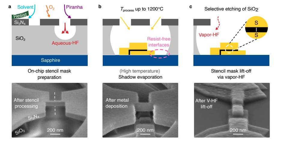
Researchers have developed a new method for fabricating superconducting quantum devices that overcomes limitations of traditional resist-based lithography. This innovative approach utilizes an on-chip stencil mask made from silicon dioxide and silicon nitride, which withstands aggressive cleaning and high-temperature processing, reaching up to 1200°C, enabling improved surface preparation and material exploration. This is crucial for minimizing defects and enhancing the coherence of superconducting qubits. The team successfully fabricated aluminum-based transmon qubits using this technique. Following metal deposition through the stencil, the mask is removed using vapor hydrofluoric acid, which selectively etches the silicon dioxide without damaging the newly formed qubit.
Devices fabricated using this method exhibited coherence times, specifically T1 relaxation times, of approximately 75 microseconds for one device and 44 microseconds for another, measured across a 200 MHz frequency range. This new method addresses key drawbacks of polymer-based lithography, which limits pre-growth cleaning and high-temperature processing due to the fragility of the resist. The inorganic stencil allows for more thorough substrate preparation, reducing amorphous layers, oxidation, and residual resist, all factors that can degrade qubit coherence. Furthermore, the on-chip design ensures precise alignment and avoids misalignment issues seen in off-chip stencil methods, promising improved reproducibility and scalability for future quantum device fabrication. This advancement paves the way for more robust and higher-performing superconducting qubits, potentially accelerating progress in quantum computing.
Inorganic Stencils Fabricate Millisecond Coherence Qubits
This work demonstrates a novel inorganic stencil lithography technique for fabricating Josephson junction qubits, offering an alternative to conventional methods that rely on organic resists. The researchers successfully developed a robust mask composed of silicon dioxide and silicon nitride, which withstands aggressive cleaning and high-temperature processing, reaching up to 1200°C. This resilience enables greater flexibility in material exploration and interface optimisation during qubit fabrication. Validation of the technique involved creating aluminum-based transmon qubits, achieving coherence times of up to several milliseconds in multiple cool-downs, confirming compatibility with state-of-the-art quantum devices.
The key advantage of this approach lies in the elimination of polymer resists from the critical fabrication steps, addressing limitations associated with contamination and thermal instability. The inorganic mask allows for a cleaner, more reliable process, and the ability to withstand high temperatures opens possibilities for additional surface treatments before deposition. While the current study focuses on aluminum-based qubits, the authors acknowledge that further research is needed to explore the technique’s applicability to other superconducting materials and junction designs. They also note the importance of optimising film deposition and surface cleaning techniques to further enhance qubit performance and coherence. This new method provides a promising pathway towards more reproducible and advanced quantum circuit fabrication.
🗞 On-chip stencil lithography for superconducting qubits
🧠 DOI: https://doi.org/10.48550/arXiv.2507.17005


