The behaviour of magnetic vortices within superconducting materials dictates their potential in diverse applications, from lossless energy transmission to highly sensitive magnetic field sensors. Understanding the mechanisms that impede, or ‘pin’, these vortices is therefore crucial for optimising device performance. A. Yu. Aladyshkin, R. A. Hovhannisyan, and colleagues report on a novel technique for visualising these pinning landscapes in granular niobium films, comparing the established method of magnetic force microscopy with their newly developed scanning quantum-vortex microscopy. Their research, detailed in the article ‘Magnetic force microscopy versus scanning quantum-vortex microscopy: Probing pinning landscape in granular niobium films’, demonstrates how a dragged vortex effectively functions as a nanoscale probe, revealing structural defects and grain boundaries with resolutions approaching the superconducting coherence length. The team, affiliated with institutions including the Moscow Institute of Physics and Technology and ESPCI Paris – PSL, present a comparative analysis of these methodologies for characterising vortex pinning potentials.
Superconductivity, characterised by zero electrical resistance and the expulsion of magnetic fields, fundamentally relies on the behaviour of Abrikosov vortices within type-II superconductors. These vortices penetrate the material and are subject to pinning forces exerted by structural defects, which are crucial for maintaining superconductivity under high currents; optimising these pinning mechanisms directly impacts the critical current density—the maximum current a superconductor can carry without losing its superconducting properties. Researchers actively investigate how defects can be engineered to enhance vortex pinning and improve superconducting performance, seeking to understand the complex interplay between vortices and the material’s microstructure.
The interaction between vortices and defects presents a significant challenge, as pinning occurs through various mechanisms involving changes in both the energy of supercurrents and the energy within the vortex cores themselves. Modern technological advancements allow for precise control over vortex pinning through techniques like sample thickness modulation and surface decoration with magnetic nanoparticles, demanding detailed knowledge of the parameters governing the pinning network.
Traditional microscopy techniques, while capable of visualising structural defects at the nanoscale, often fall short in comprehensively characterising vortex pinning. Transmission electron microscopy is destructive and examines only a small sample volume, while scanning probe microscopy techniques, such as atomic force microscopy, primarily reveal surface features and provide limited information about the internal properties of defects. This highlights the need for a technique capable of nanoscale resolution, a wide field of view, low-temperature operation, and non-destructive measurement.
Recent developments focus on utilising the vortices themselves
Recent developments focus on utilising the vortices themselves as probes to investigate pinning potentials, offering a promising avenue for understanding the complex interplay between defects and vortices. This approach, detailed in the development of scanning-vortex microscopy, allows for visualisation of grain boundaries and characterisation of pinning potentials with resolutions approaching the superconducting coherence length—a fundamental parameter governing the behaviour of superconducting materials, representing the distance over which superconducting electrons maintain correlation.
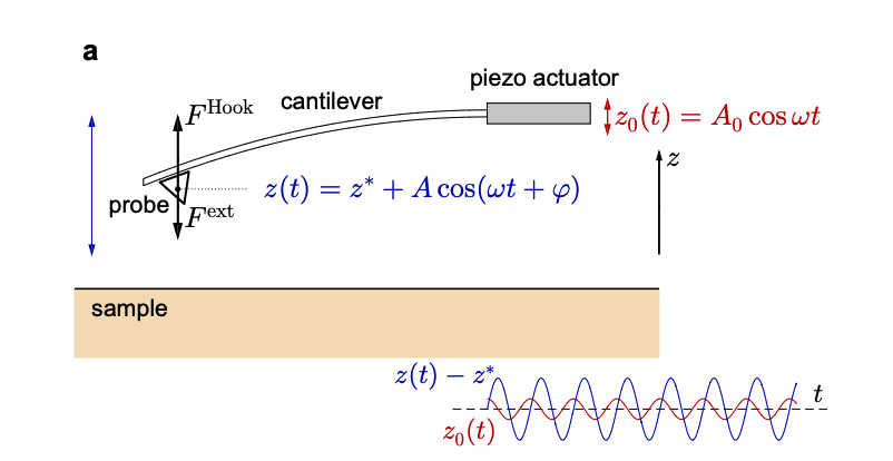
This technique builds upon established principles of magnetic force microscopy, but introduces a crucial dynamic element: the active manipulation and tracking of individual magnetic vortices. Traditional magnetic force microscopy passively images the magnetic landscape of a material, revealing the presence of vortices as localised disturbances in the magnetic field; however, this new approach actively utilises the magnetic tip of the cantilever to capture and drag a single vortex across the sample surface.
This is achieved by carefully controlling the scanning parameters as the temperature approaches the critical temperature of the niobium film, where the pinning forces exerted by structural defects weaken, allowing the magnetic tip to overcome them. The principle hinges on a delicate balance of forces, as the dragged vortex does not simply follow the path dictated by the cantilever, but continues to interact with the underlying structural defects within the niobium film.
These interactions serve as a sensitive probe of the pinning potentials present in the material, effectively transforming the vortex into a nanoscale explorer, allowing researchers to map the distribution and strength of these pinning potentials with a resolution of approximately 30 nanometres. This resolution is comparable to the superconducting coherence length and represents a significant advancement over traditional magnetic force microscopy, which is often limited by the size of the magnetic tip and the difficulty in distinguishing between genuine pinning sites and artefacts.
The use of magnetron-sputtered niobium films is central to this methodology, as magnetron sputtering is a physical vapour deposition technique that allows for the creation of thin films with controlled composition and microstructure. The resulting granular structure of these films, containing numerous grain boundaries and defects, provides the necessary pinning sites for the magnetic vortices, influencing the critical current that a superconductor can carry without losing its superconducting properties.
The research presents a novel technique, scanning-vortex microscopy, for investigating vortex pinning in superconducting films and nanodevices, utilising magnetron-sputtered niobium films and low-temperature magnetic force microscopy to characterise their magnetic properties. As temperature nears the critical temperature for superconductivity, the study demonstrates a weakening of pinning potential caused by structural defects, allowing the magnetic tip of the cantilever to trap and drag individual vortices during scanning. The dragged vortex functions as a nanoscale probe, interacting with structural defects and revealing pinning potentials, visualising grain boundaries within granular niobium films with a resolution of approximately 30 nanometres.
This technique effectively utilises the vortex itself as
This technique effectively utilises the vortex itself as a sensitive indicator of the local pinning landscape, demonstrating that the magnetic interaction between the tip and a single vortex dominates as the temperature nears the critical point, enabling the controlled manipulation and imaging of these vortices. The study highlights the potential of scanning-vortex microscopy to provide insights into the nanoscale behaviour of vortices and the influence of microstructural features on their pinning.
The study highlights the sensitivity of the technique to subtle variations in the pinning landscape, offering insights into the interplay between material microstructure and superconducting properties. Even in seemingly defect-free samples, the Earth’s magnetic field can induce vortex formation, a crucial consideration for accurate magnetic force microscopy measurements. The use of lateral Josephson junctions as magnetic sensors further enhances the precision and sensitivity of the vortex imaging process, contributing to a deeper understanding of superconductivity in thin films.
Future work should focus on extending this methodology to investigate more complex superconducting materials and nanostructures, exploring the influence of varying film thicknesses, deposition parameters, and defect densities on vortex behaviour. Investigating the dynamic response of vortices to applied currents and magnetic fields would provide valuable insights into the critical current limitations of superconducting devices. Expanding the technique to three-dimensional imaging, potentially through the integration of tomographic methods, could offer a more complete picture of vortex distribution and pinning landscapes. Finally, applying scanning-vortex microscopy to study the behaviour of vortices in high-temperature superconductors could reveal new insights into the mechanisms governing superconductivity in these complex materials, potentially paving the way for the development of advanced superconducting technologies.
🗞 Magnetic force microscopy versus scanning quantum-vortex microscopy: Probing pinning landscape in granular niobium films
🧠 DOI: https://doi.org/10.48550/arXiv.2507.05172


