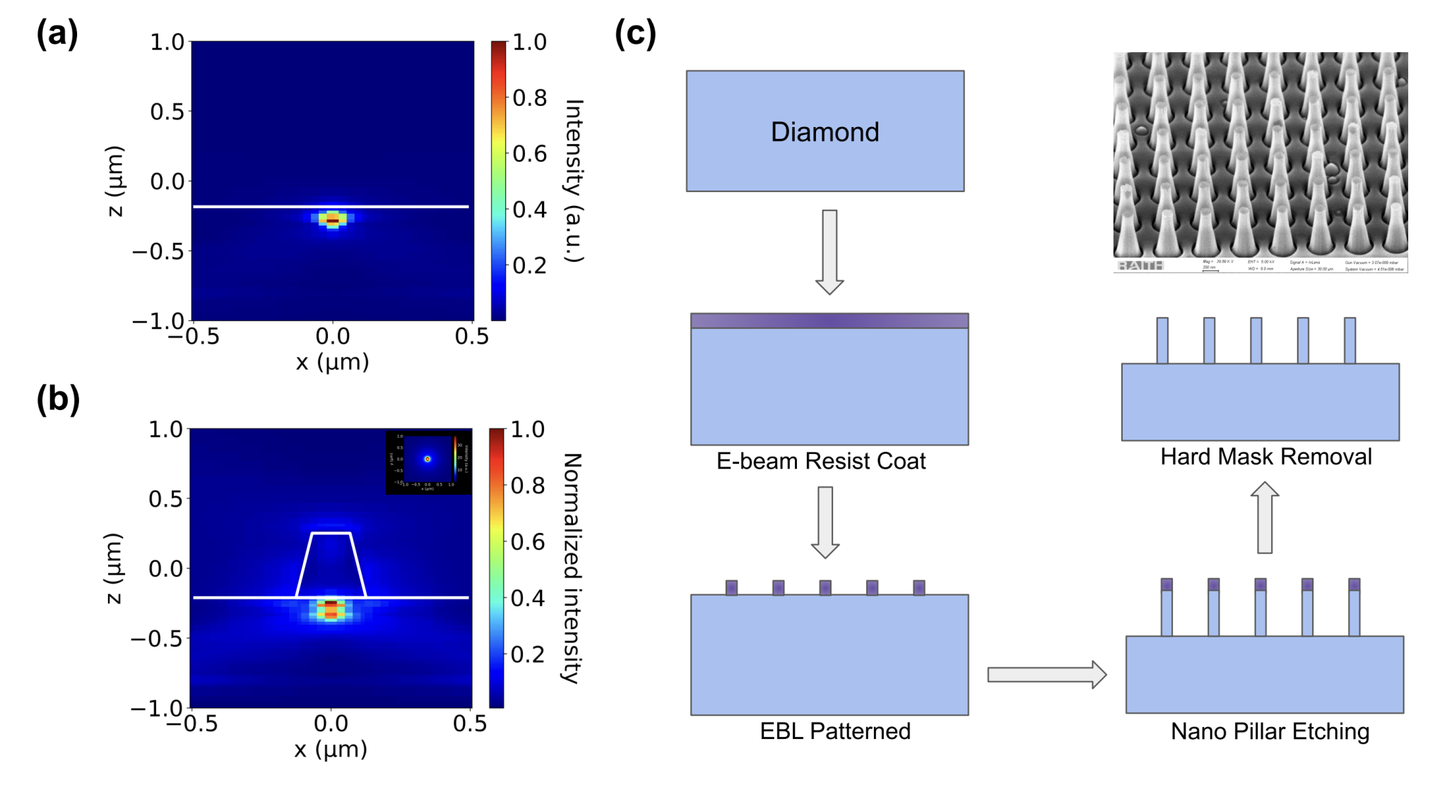
Diamond’s unique properties increasingly position it as a leading material for nanoscale technologies, and researchers are now meticulously investigating how to build complex devices within it. Ayan Majumder from the Indian Institute of Technology Bombay, Vivek K Shukla from the University of Mumbai, and Anuj Bathla from the Indian Institute of Technology Bombay, alongside colleagues, have focused on the subtle effects of manufacturing processes on these delicate structures. Their work demonstrates that creating nanophotonic devices in diamond inevitably introduces strain into the crystal lattice, and this strain significantly alters the behaviour of key quantum properties within the material. By carefully analysing these changes using a technique called optically detected magnetic resonance, the team reveals a method for both measuring and understanding the strain, offering a crucial step towards building reliable and scalable quantum technologies based on diamond.
Nitrogen-vacancy (NV−) centers and other colour centres in diamonds are promising platforms for quantum communication, quantum information processing, and nanoscale sensing, owing to their long spin coherence times, fast spin control, and efficient photon coupling. Precisely controlling and manipulating these centres is crucial for practical quantum technologies, yet achieving deterministic placement of these defects remains a significant challenge. Researchers are therefore exploring techniques to overcome these limitations and unlock the full potential of diamond as a quantum material. This work focuses on developing a method for the deterministic placement of colour centres, which would represent a substantial advancement in the field.
Boron Implantation and NV Center Engineering
They also explore the use of photonic crystal cavities to enhance the interaction between NV centers and photons, improving the efficiency of quantum operations. The observation of anti-bunching, a phenomenon where photons are emitted one at a time, confirms the single-photon emission properties of the NV centers, crucial for applications in quantum communication and quantum cryptography. The research also investigates how the conditions used to grow diamond films, using a technique called chemical vapor deposition (CVD), affect nitrogen incorporation and defect formation, providing further control over NV center properties.
Nitrogen Vacancy Centers Map Diamond Strain
Researchers have demonstrated a sensitive method for characterizing strain within diamond crystals, leveraging the unique properties of nitrogen-vacancy (NV) centers. The team investigated how ion implantation and nanofabrication processes induce strain, which can significantly impact the performance of diamond-based nanophotonic devices. Experiments reveal that zero-field continuous-wave optically detected magnetic resonance (CW-ODMR) spectroscopy serves as a powerful probe of local crystal strain, providing both quantitative and directional information about these stresses. The study involved implanting nitrogen ions into single-crystal diamond samples at specific energies and doses.
Simulations predicted the resulting concentration of vacancies within the diamond lattice, showing how the implantation process creates defects at a specific depth below the surface. The calculated damage, expressed as vacancy concentration, varied with the ion dose, providing a clear understanding of the defect creation process. Analysis of the zero-field ODMR spectra revealed an asymmetric splitting, which the researchers linked to strain-induced modifications in the spin Hamiltonian of the NV centers. This asymmetry provides a means to characterize the magnitude and direction of strain within the diamond crystal. The team developed a theoretical model to explain these spectral features, offering a framework for characterizing strain effects in diamond-based nanophotonic devices and paving the way for improved device design and performance. This advancement is crucial for realizing the full potential of diamond as a platform for quantum technologies and nanoscale applications.
Crystal Strain Impacts NV Center Spin Levels
This research demonstrates that crystal strain significantly affects the electronic spin levels of nitrogen-vacancy (NV) centers in diamond, a crucial consideration for their application in quantum technologies. Researchers observed asymmetric splitting in the zero-field optically detected magnetic resonance (ODMR) spectrum of both nitrogen ion-implanted and diamond nanopillar samples, directly linking this effect to shear strain within the diamond lattice. They developed a model to explain and quantify these observations, providing a means to characterize strain components and their impact on NV center performance. The ability to accurately assess crystal strain is vital for optimizing diamond-based devices used in quantum communication, sensing, and information processing.
This method offers a valuable tool for understanding qubit coherence, calibrating quantum gates, and improving the optical properties of emitted photons, ultimately enhancing the performance of these emerging technologies. The authors acknowledge that increasing ion implantation doses can lead to greater lattice distortion, and future work could focus on minimizing these effects to further refine device fabrication. This research provides a framework for assessing and optimizing device performance across various quantum platforms, contributing to the advancement of this field.
🗞 Characterization of Strain Parameters in a Diamond Nanophotonic Structure
🧠 ArXiv: https://arxiv.org/abs/2508.16335


