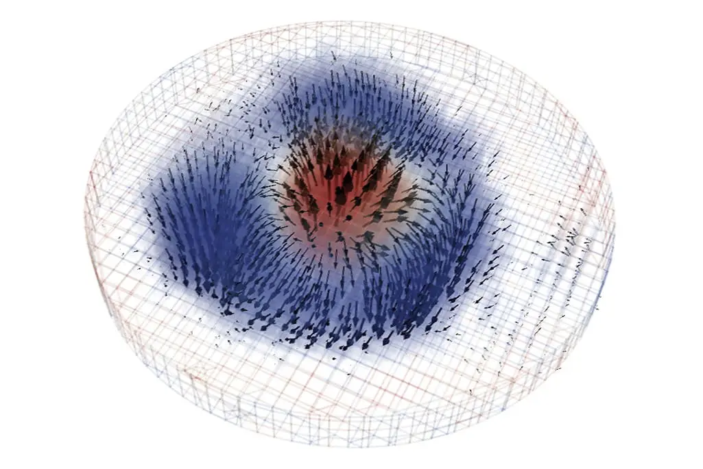
Researchers have successfully taken three-dimensional X-ray images of a nanoscale object called a magnetic skyrmion, which could lead to breakthroughs in microelectronic storage devices and quantum computing.
The team, led by Peter Fischer, a senior researcher at Lawrence Berkeley National Laboratory, used a novel imaging technique called magnetic X-ray laminography to characterize the spin structures within the entire 3D object. This achievement provides a foundation for nanoscale metrology in spintronics devices, which could enable massive data storage while consuming much less power.
Magnetic skyrmions are stable, small, and fast, with spin directions that can carry and store information, similar to how electrons work in current devices.
The DOE Office of Science supported the research and involved collaboration with Western Digital and the Molecular Foundry’s nanofabrication facility.
Unveiling the 3D Structure of Magnetic Skyrmions: A Breakthrough for Spintronics Devices
Magnetic skyrmions, nanoscale spinning circles of magnetism, have long been considered a promising material for future microelectronic devices, including quantum computers. However, researchers need a deeper understanding of these complex objects to harness their potential. Recently, a team led by Peter Fischer at the Lawrence Berkeley National Laboratory (Berkeley Lab) has successfully taken 3D X-ray images of skyrmions, providing a foundation for nanoscale metrology in spintronics devices.
Magnetic skyrmions are characterized by their unique spin structure, where the magnetic spin at the center points upward, while moving out from the center, the magnetism twists and pulls in a downward direction. This topological stability makes them attractive for carrying and storing information in microelectronic devices. Unlike current devices that rely on the charge of electrons, which comes with inevitable energy losses, skyrmions could potentially reduce these losses significantly.
The Limitations of 2D Descriptions
Theoretical knowledge of skyrmions has been based on descriptions of them as 2D objects. However, in the real world of electronics and silicon wafers, skyrmions must be dealt with as 3D objects. To put skyrmions to work or synthesize custom skyrmions, researchers must be able to examine and understand their spin characteristics throughout the whole 3D object.
To overcome this limitation, David Raftrey, a student researcher in Fischer’s team, used a novel imaging technique called magnetic X-ray laminography at the Swiss Light Source. By taking a thin magnetic layer synthesized by colleagues from Western Digital and patterning a nanodisk using the Molecular Foundry’s nanofabrication facility, Raftrey was able to obtain 3D tomographic images of the skyrmion. This process took months, finally yielding a better understanding of skyrmion spin structures.
Implications for Spintronics Devices
A full understanding of skyrmions’ 3D spin texture “opens opportunities to explore and tailor 3D topological spintronic devices with enhanced functionalities that cannot be achieved in two dimensions,” Fischer said. This breakthrough has significant implications for the development of microelectronic devices, including quantum computers, which could potentially benefit from the unique properties of skyrmions.
The Molecular Foundry is a DOE Office of Science user facility at Berkeley Lab, where researchers from around the world rely on its world-class scientific facilities for their own pioneering research. The work was supported by the DOE Office of Science, which is committed to addressing some of the most pressing challenges of our time through basic research in the physical sciences.
External Link: Click Here For More


