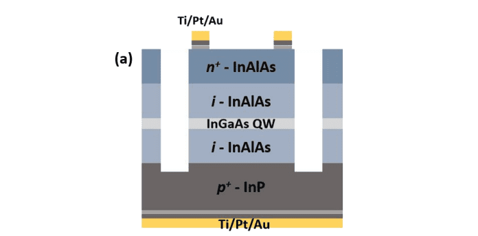
Research into quantum well solar cells demonstrates that wider quantum wells exhibit stronger hot carrier effects, correlating with increased quasi-Fermi level splitting. Open-circuit voltage aligns with confinement degree, however, photocurrent generation primarily occurs within the barrier layer, indicating minimal carrier contribution from the quantum wells themselves.
The pursuit of more efficient solar energy conversion continually drives research into novel semiconductor structures, with hot carrier solar cells representing a promising avenue beyond the Shockley–Queisser limit. These devices aim to harness the energy of photogenerated carriers before it dissipates as heat, requiring precise control over carrier confinement and thermodynamic properties within nanoscale materials. Nil Selen Aydin, Leopold Rothmayer, and colleagues from the Technical University of Munich, alongside Gregor Koblmüller from the Technical University Berlin, investigate these phenomena in a study entitled ‘Unraveling Quantum Size-Dependent Optoelectrical Phenomena in Hot Carrier Quantum Well Structures’. Their research focuses on the impact of varying quantum well thickness on hot carrier behaviour within InGaAs/InAlAs heterostructures, revealing a complex interplay between confinement, quasi-Fermi level splitting, and photocurrent generation.
The behaviour of high-energy carriers, known as hot carriers, within indium gallium arsenide/indium aluminium arsenide (InGaAs/InAlAs) heterostructure diodes is significantly influenced by the thickness of the quantum wells (QWs) incorporated into their design. This research investigates the thermodynamic and optical properties of these carriers across QW widths of 4 nm, 5.5 nm, and 7.5 nm, demonstrating a clear correlation between QW thickness and the strength of observed hot carrier effects. Quantum wells are semiconductor structures that confine electrons, protons and holes to a small region, creating quantised energy levels.
The study reveals that increased QW thickness, specifically at 7.5 nm, enhances the generation and preservation of hot carriers within the potential wells. This is evidenced by a corresponding increase in the open-circuit voltage, which aligns with the degree of quantum confinement and mirrors the splitting of quasi-Fermi levels, a measure of carrier distribution. However, measured voltages exceeding the material’s bandgap suggest the barrier layer, the surrounding semiconductor material, plays a crucial role, potentially through carrier accumulation or altered band bending, necessitating further investigation into its characteristics. Band bending refers to the distortion of energy bands within a semiconductor due to external influences.
Detailed optical analysis, utilising photoluminescence spectroscopy – a technique that examines the light emitted by a material – confirms the impact of QW thickness on exciton localisation. Excitons are bound electron-hole pairs within a semiconductor. The full width at half maximum (FWHM) of the photoluminescence peak, a measure of spectral broadening, decreases as QW thickness increases, indicating a relationship between exciton localisation energy and interface roughness. The data demonstrates a linear dependence between FWHM and the inverse square of the QW thickness, supporting this connection. Absorption characteristics remain consistent across samples, except for the 7.5 nm QW, which exhibits distinct absorption features in both the potential well and barrier regions.
Notably, the short-circuit current, a measure of the current generated by light, exhibits a strong dependence on excitation power, but remains largely unaffected by the degree of quantum confinement. This suggests that the majority of photocurrent originates within the barrier layer, with minimal contribution from photogenerated carriers residing within the QWs themselves. This finding indicates that efficient extraction of hot carriers from the wells remains a significant challenge.
The study provides a foundation for further exploration of QW structures in the context of hot carrier solar cells, with investigations into interface quality, barrier layer composition, and device architecture being crucial to unlock their full potential for enhancing power conversion efficiency. Understanding and controlling carrier dynamics within both the wells and barriers represents a key step towards realising high-performance optoelectronic devices.
👉 More information
🗞 Unraveling Quantum Size-Dependent Optoelectrical Phenomena in Hot Carrier Quantum Well Structures
🧠 DOI: https://doi.org/10.48550/arXiv.2507.04112


