Creating nanoscale sensors with diamond presents a significant challenge, as conventional fabrication techniques often damage the delicate quantum properties within the material. Alexander Pakpour Tabrizi, Artur Lozovoi, and Sean Karg, all from Princeton University, alongside colleagues including Tecla Bottinelli Montandon and Melody Leung, now demonstrate a new method for creating high-quality nanostructured diamond membranes. Their approach minimises subsurface damage and surface defects, preserving the optical and spin properties of nitrogen-vacancy centres located extremely close to the diamond surface, and even enhancing their sensitivity. This breakthrough enables the creation of highly sensitive nanoscale sensors and facilitates their integration with a wide range of materials, paving the way for advancements in condensed matter physics and materials science.
Detailed Methods, Simulations and Data Analysis
This document provides a comprehensive overview of the methods, simulations, and data analysis underpinning a recent research study, allowing other researchers to understand and build upon this work. It details the experimental setup, simulation parameters, and data processing techniques used to achieve the reported findings. The supplementary materials detail computational modeling used to understand light collection efficiency from nitrogen-vacancy (NV) centers in nanobeams, revealing a preference for wider, thinner structures and the impact of positioning the nanobeam on a sapphire substrate. Further analysis focused on detailed experimental procedures, including laser pulse sequences and methods for determining the charge state of NV centers, demonstrating a correlation between charge state and spin contrast.
Key takeaways emphasize the importance of optimizing light collection efficiency and the significant impact of nanobeam geometry on performance. Computational modeling proved vital in understanding the interplay between light, nanobeam geometry, and NV center properties, while rigorous data analysis techniques extracted meaningful insights from measurements. Potential areas for future research include investigating fabrication imperfections, exploring surface effects on NV center stability, developing methods for dynamic charge control, and integrating NV centers with other quantum circuit elements.
Nanomembrane Fabrication via Modified Reactive Etching
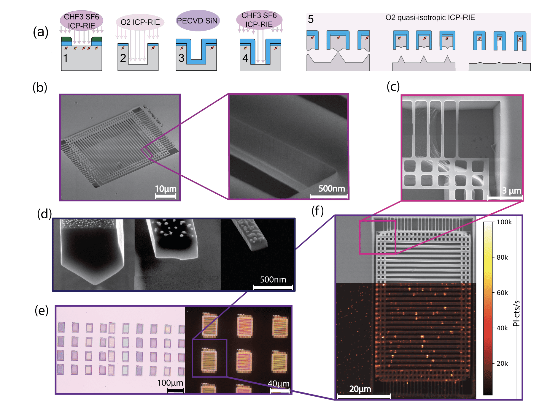
Researchers have engineered a novel fabrication process for low-damage nanostructured diamond membranes, crucial for positioning nitrogen-vacancy (NV) centers close to sensing targets. The process adapts the single crystal reactive etching and metallization (SCREAM) technique for diamond, utilizing anisotropic and quasi-isotropic etching at lower temperature and power to create a diffuse plasma that etches different crystallographic directions at varying rates. By carefully controlling etching parameters, researchers achieved uniform undercutting across microns of dense nanostructures, enabling precise control over beam and tether thicknesses. Sacrificial tethers connect the nanostructures to the host substrate, balancing mechanical stability with eventual separation. The resulting nanobeam membranes host NV centers within nanometers of the surface, exhibiting state-of-the-art nanoscale sensing performance, and collection efficiency is enhanced up to seven-fold when integrated with a sapphire target.
Low-Damage Nanodiamond Membranes Preserve NV Center Properties
Scientists have developed a new method for fabricating low-damage nanostructured diamond membranes, preserving the optical and spin properties of shallow nitrogen-vacancy (NV) centers located near the diamond surface. This breakthrough enables the creation of nanoscale sensing platforms with enhanced performance for applications in condensed matter physics and materials science. Researchers successfully fabricated membranes with nanobeam widths ranging from 120 to 720 nanometers, achieving near-vertical sidewalls and minimized edge collapse. Measurements confirm that the spin coherence time, charge state stability, and charge dynamics of shallow NV centers within these nanobeams are comparable to those found in bulk diamond substrates. The nanobeam form factor significantly enhances collection efficiency, with an observed increase of up to a factor of seven when integrated with a sapphire target. A pick-and-place transfer method enables seamless integration of these nanobeams with diverse sensing targets, yielding high-yield, transferable nanobeam frames with individual nanobeams as narrow as 100 nanometers.
Diamond Nanomembrane Sensing Platform Demonstrated
This research establishes a practical platform for quantum sensing experiments by fabricating low-damage nanostructured diamond membranes hosting high-performance, shallow nitrogen-vacancy (NV) centers. The team successfully demonstrated a fabrication process that preserves the optical and spin properties of these NV centers, even when positioned very close to the diamond surface, while simultaneously enhancing photon collection through careful membrane structuring. Researchers also developed a pick-and-place transfer method, enabling seamless integration of these diamond nanostructures with diverse sensing targets, including materials that are optically opaque. The resulting devices exhibit enhanced collection efficiency and require reduced excitation power, improving measurement speed and minimizing illumination of the sample being studied. Future work could focus on patterned implantation of NV centers using nanopatterning techniques and extending this fabrication process to create low-dimensional diamond structures like nanosheets and nanowires.
👉 More information
🗞 High-quality nanostructured diamond membranes for nanoscale quantum sensing
🧠 ArXiv: https://arxiv.org/abs/2511.08632


